Photoelectric sensor, optical module and method of producing same

A photoelectric sensor, optical module technology, applied in semiconductor/solid-state device manufacturing, optics, optical components, etc., can solve problems such as reduced yield, large changes in light behavior, and damage to lenses

Inactive Publication Date: 2007-04-25
ORMON CORP
View PDF4 Cites 9 Cited by
  • Summary
  • Abstract
  • Description
  • Claims
  • Application Information

AI Technical Summary

Problems solved by technology

Therefore, if there is a positional deviation between them, the variation in the behavior of the generated light becomes large to cause a problem of lower yield
[0017] Another problem is that as the lens becomes thinner, if an eject pin is used to remove the lens from the mold when it is manufactured by injection molding, the eject pin is likely to penetrate and damage the lens

Method used


Image

  • Photoelectric sensor, optical module and method of producing same
  • Photoelectric sensor, optical module and method of producing same
  • Photoelectric sensor, optical module and method of producing same

Examples


Embodiment Construction

[0047] The present invention will be described below through an example, wherein the present invention is applied to a light projector and a light receiver of a photoelectric sensor as an optical module. In the examples described, the same components are denoted by the same reference numerals, and their descriptions will not be repeated.

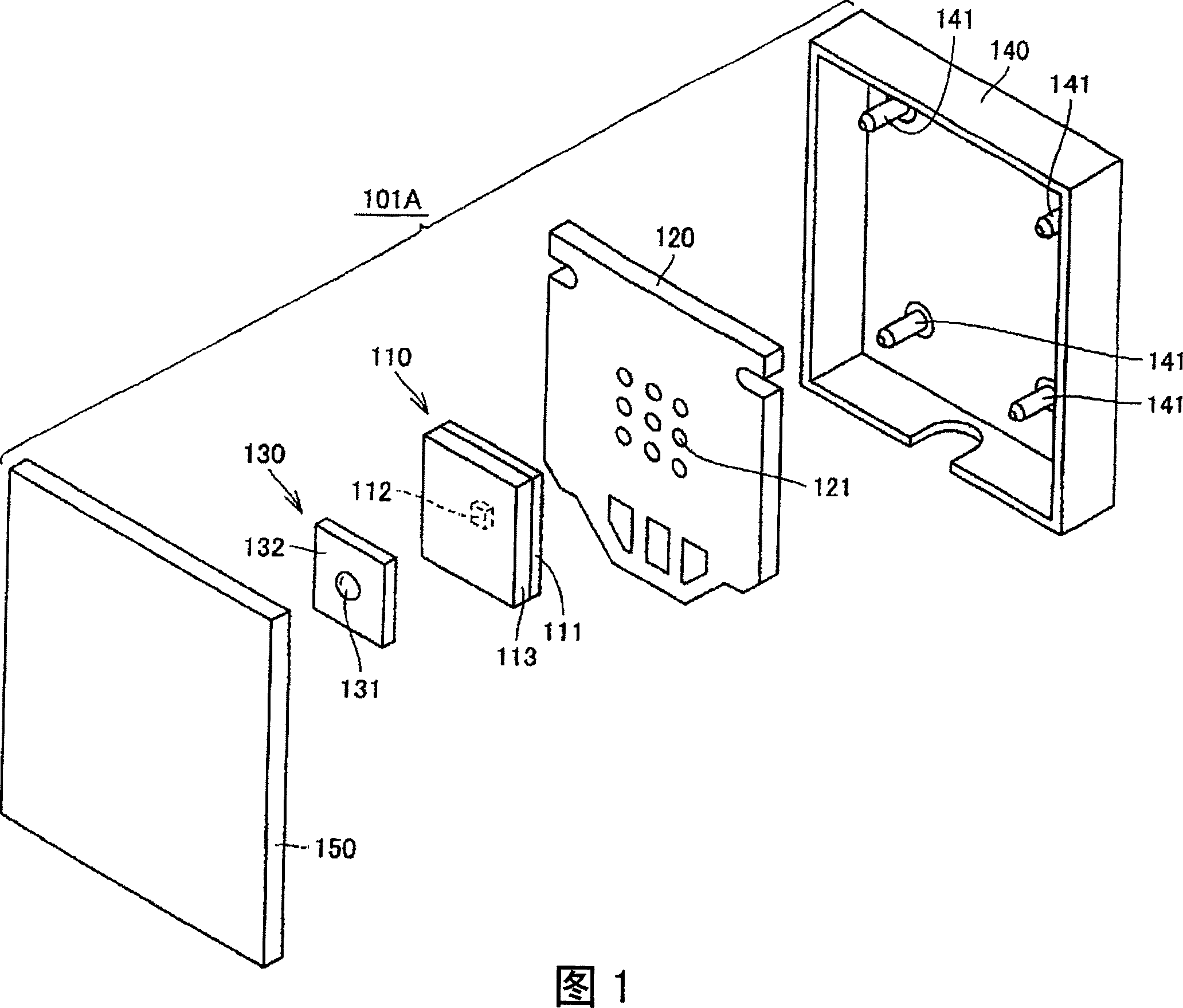
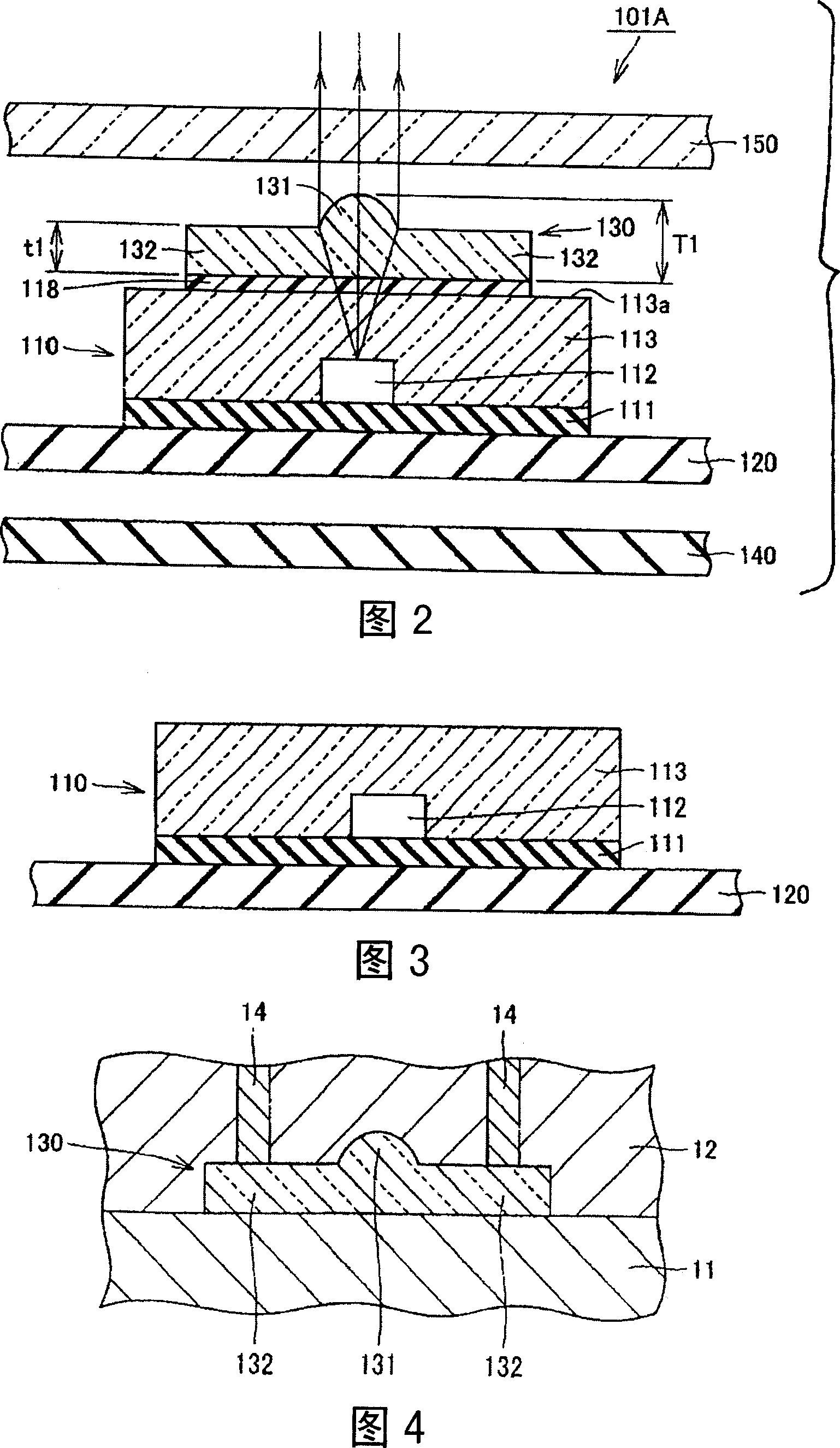
[0048] FIG. 1 is an exploded perspective view of a light projector 101A according to a first embodiment of the present invention, and FIG. 2 is a partial cross-sectional view of the assembled light projector 101A. The structure of the light projector 101A will be described below with reference to FIGS. 1 and 2 .

[0049] As shown in FIGS. 1 and 2 , the light projector 101A according to the first embodiment of the present invention includes an IC package 110 in the form of a CSP, a mounting substrate 120 , a lens unit 130 , a housing 140 and a cover 150 . A CSP-type IC package 110 includes an intermediate substrate 111 , an LED 112 as a semi...


PUM


Abstract

An optical module is formed with a semiconductor optical element sealed inside a transparent resin part and a lens unit affixed to its upper surface. The-lens unit has a lens part that is disposed facing opposite the semiconductor optical element through the transparent resin part. A planar part extends from the lens part along the upper surface of the transparent resin part. A photoelectric sensor may include such an optical module as a light projector and another such optical module as a light receiver.

Description

[0001] This application claims priority from Japanese Patent Application No. 2005-304759 filed on October 19, 2005. technical field [0002] The present invention relates to an optical module, such as a light projection and receiving unit of a photoelectric sensor, and to a method of manufacturing such an optical module and a photoelectric sensor having such an optical module. Background technique [0003] Regarding an optical module of a photosensor for object detection, it is necessary to combine a semiconductor optical element such as a light emitting diode (LED), a laser diode (LD) or a photodiode (PD) with the above semiconductor optical element such as a light projection lens or a light receiving lens, etc. The position of the element corresponding to the set lens is precisely matched. If this position matching is not achieved with sufficient precision, projection or reception of light will not proceed as intended, and detection of objects will not be accurately achiev...

Claims


Application Information

Patent Timeline
Patent Type & Authority Applications(China)
IPC IPC(8): H01L33/00H01L31/00H01L31/0203H01L31/18H01L25/16H01L25/00H01L21/50G01C3/00G02B6/00G02B3/00H01L33/58
CPCH01L31/0203H01L31/18H01L33/58H01L31/0232H01L2924/0002H01L31/02325H01L2924/00
Inventor 奥浓基晴杉本诚小谷慎二郎
Owner ORMON CORP
Why Eureka
Try Eureka