

Method for plating printed circuit board and printed circuit board manufactured therefrom
A technology of printed circuit boards and printed circuits, which is applied in the direction of printed circuit manufacturing, printed circuits, printed circuit components, etc., and can solve problems such as applications that are not suitable for low current and high frequency
Inactive Publication Date: 2007-05-02
SAMSUNG ELECTRO MECHANICS CO LTD +1
View PDF3 Cites 23 Cited by
- Summary
- Abstract
- Description
- Claims
- Application Information
AI Technical Summary
Problems solved by technology
Therefore, nickel-plated PCBs are not suitable for low-current, high-frequency applications
Method used
View moreImage
Smart ImageViewing Examples

Examples
Embodiment 1
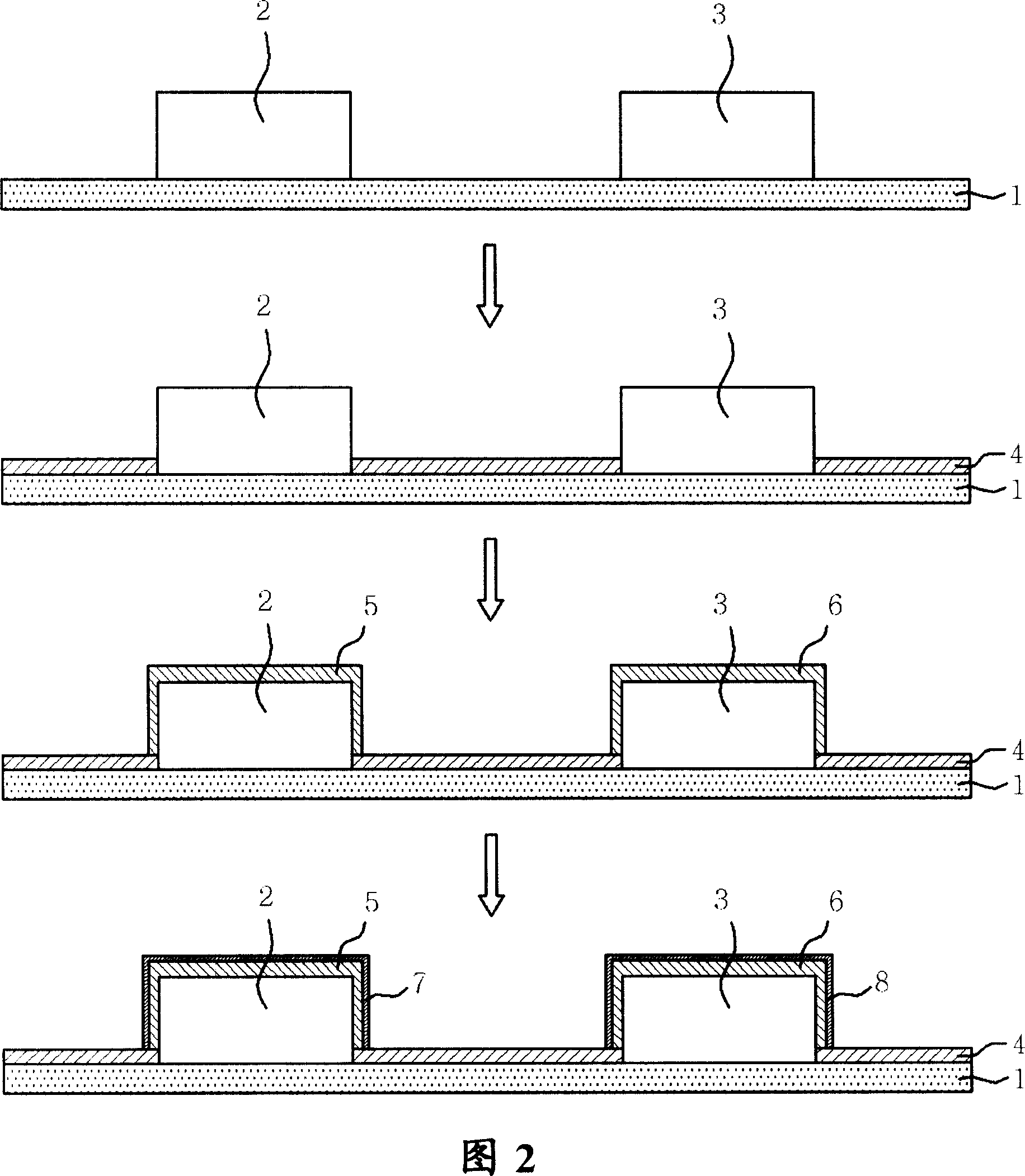
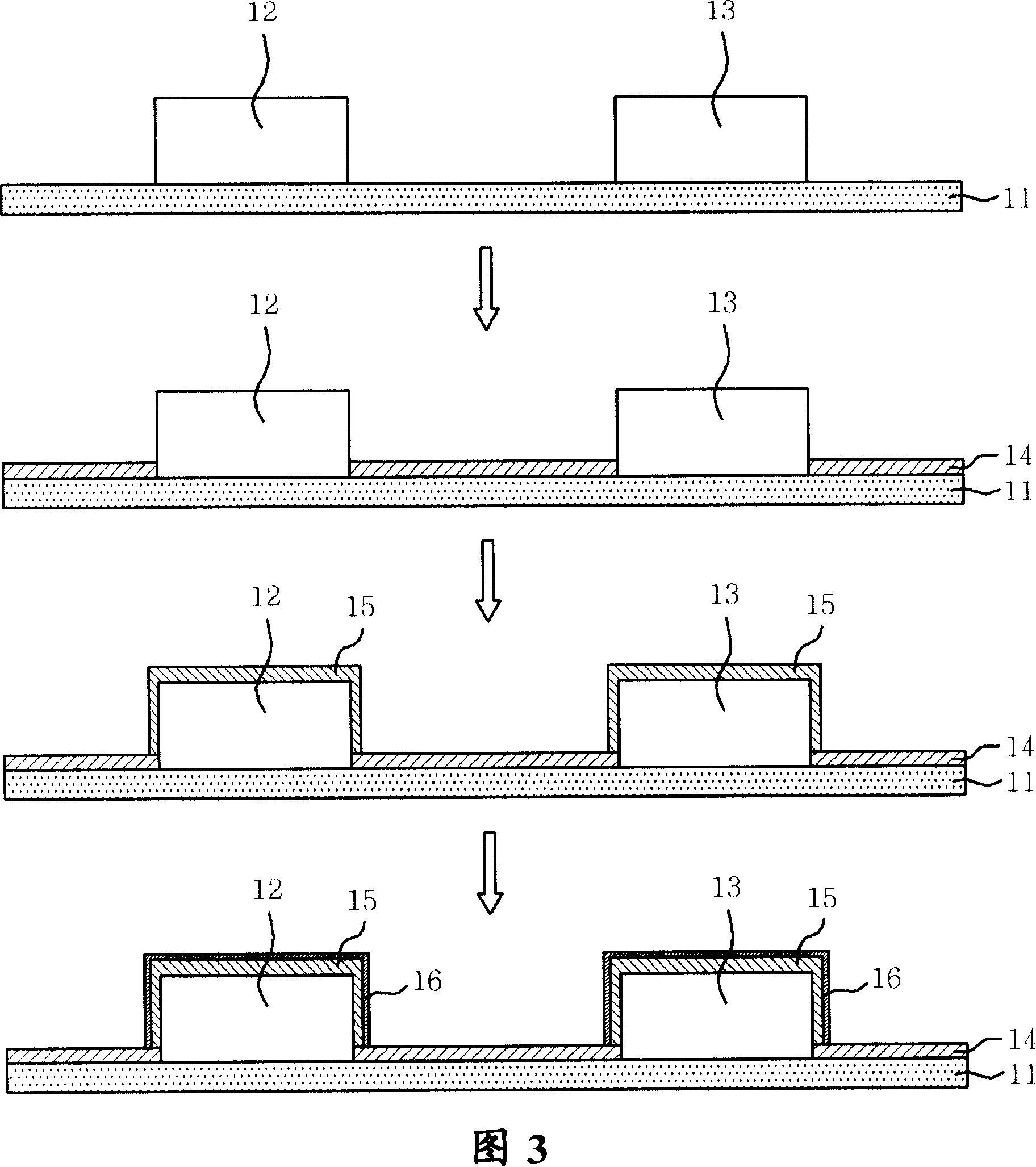
[0087] On the copper layer of the printed circuit board of pretreatment, by palladium: the ratio of phosphorus is 96.7: 3.3 (wt%) the palladium-phosphorus alloy plating that constitutes to thickness is 0.2 μ m, then forms thickness on the palladium phosphorus alloy plating layer 0.05μm gold plating.
Embodiment 2
[0089] The same procedure as in Example 1 was repeated except that a palladium-boron alloy composed of a palladium:boron ratio of 99.3:0.7 (wt%) was used instead of palladium-phosphorus.
Embodiment 3
[0091] The same procedure as in Example 1 was repeated except that pure palladium was used instead of the palladium alloy.
Login to View More PUM
| Property | Measurement | Unit |
|---|---|---|
| thickness | aaaaa | aaaaa |
| thickness | aaaaa | aaaaa |
| electrical resistivity | aaaaa | aaaaa |
Abstract
Disclosed herein are a method for plating a printed circuit board and the printed circuit board manufactured therefrom. In the method, a bare soldering or wire bonding portion of a copper (Cu)- or copper alloy layer, is plated with palladium (Pd) or a palladium alloy, and then gold (Au) or a gold alloy is deposited over the palladium or palladium alloy plated layer by an electroless substitution plating process based on ionization tendency. Having superior hardness, ductility and corrosion resistance, palladium is suitable for use between a connector and a substrate and meets requirements for the printed circuit board even when applied to a low thickness, greatly reducing the process time. Accordingly, the problem of black pad, which frequently occur on electroless nickel and electroless gold finish upon surface mount technology, can be perfectly solved. Particularly, fatal bending cracks can be prevented from occurring in the rigid-flexible or flexible printed circuit boards.
Description
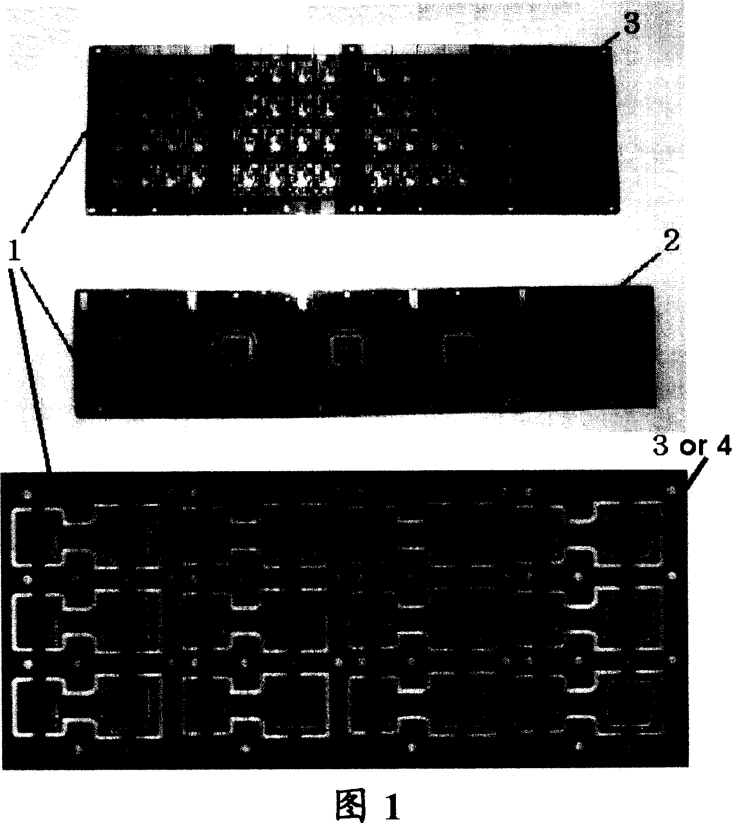
[0001] Cross References to Related Applications [0002] This application claims priority to Korean Patent Application No. 10-2005-0100787, filed Oct. 25, 2005, entitled "Method for Plating Printed Circuit Boards and Printed Circuit Boards Produced Thereby," the full text of which Incorporated into this application by reference. technical field [0003] The present invention generally relates to a method for plating printed circuit boards and printed circuit boards manufactured thereby, more particularly, the present invention relates to a method for plating printed circuit boards and printed circuit boards manufactured thereby board, wherein the method comprises forming a palladium or palladium alloy plating on bare copper in a printed circuit board by substitution plating by electroless plating and forming gold or gold alloy plating on the palladium or palladium alloy plating by substitution plating by electroless plating plating. Such a printed circuit board manufactured ...
Claims
Login to View More Application Information
Patent Timeline
 Patent Type & AuthorityApplications(China)
IPC IPC(8): H05K3/18H05K1/09H05K1/00
CPCH01L2924/0002C23C18/44H05K3/244H05K2203/073H05K2203/072C23C18/54H01L21/4846H01L23/498H05K3/28H01L24/85H01L2224/45124H01L2224/85444H01L2224/45144H01L2924/00011Y10T428/24917H01L2924/00H01L2924/01033H05K3/18
Inventor任奎赫全星郁杨德桭安东基李哲敏韩美贞
OwnerSAMSUNG ELECTRO MECHANICS CO LTD