
Heat treatment jig for silicon semiconductor substrate

一种硅基板、半导体的技术,应用在处理舟使用的领域,能够解决设备成品率降低等问题,达到维持品质特性、降低平滑裂隙、消除表面阶梯差的效果

Active Publication Date: 2007-05-23
SUMCO CORP
View PDF5 Cites 3 Cited by
  • Summary
  • Abstract
  • Description
  • Claims
  • Application Information

AI Technical Summary

Problems solved by technology

The surface step difference generated on the back of the silicon substrate causes defocusing in the photolithography process of the device manufacturing process, which greatly reduces the yield of the device

Method used

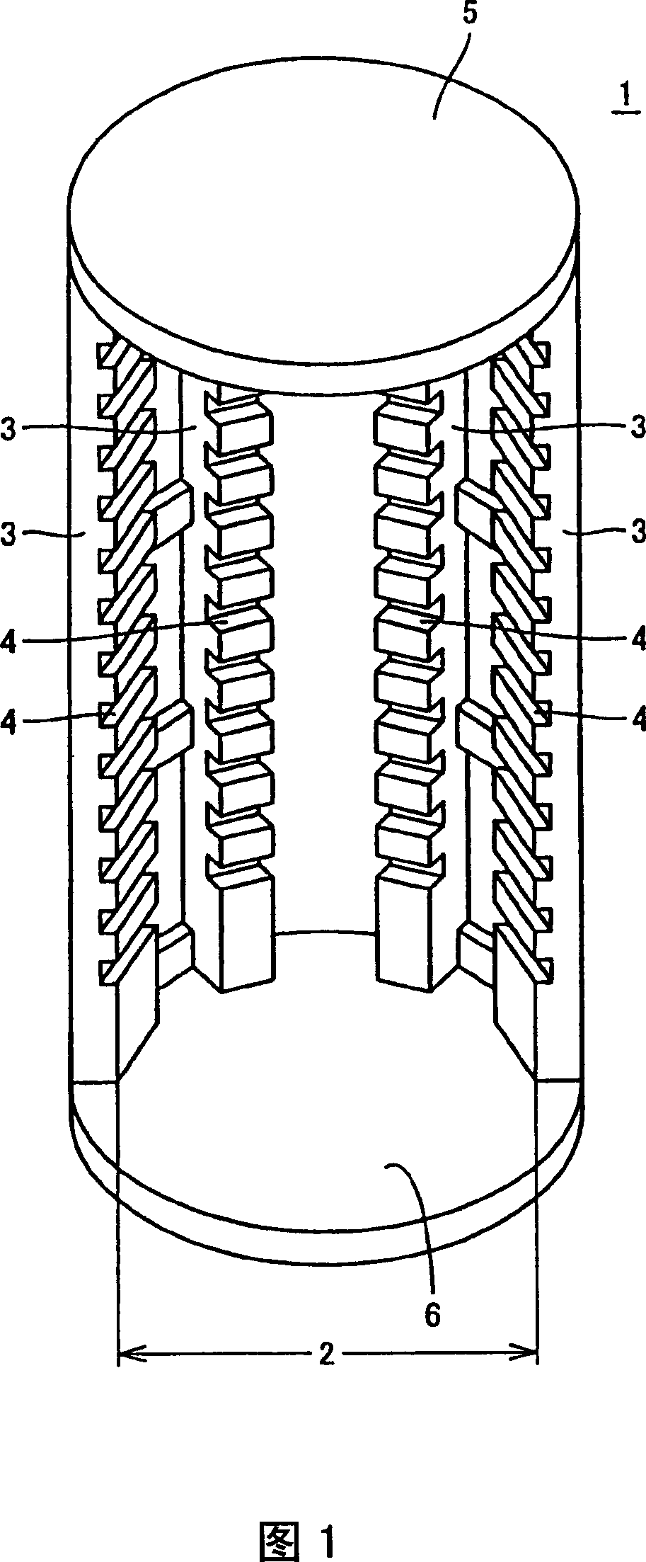
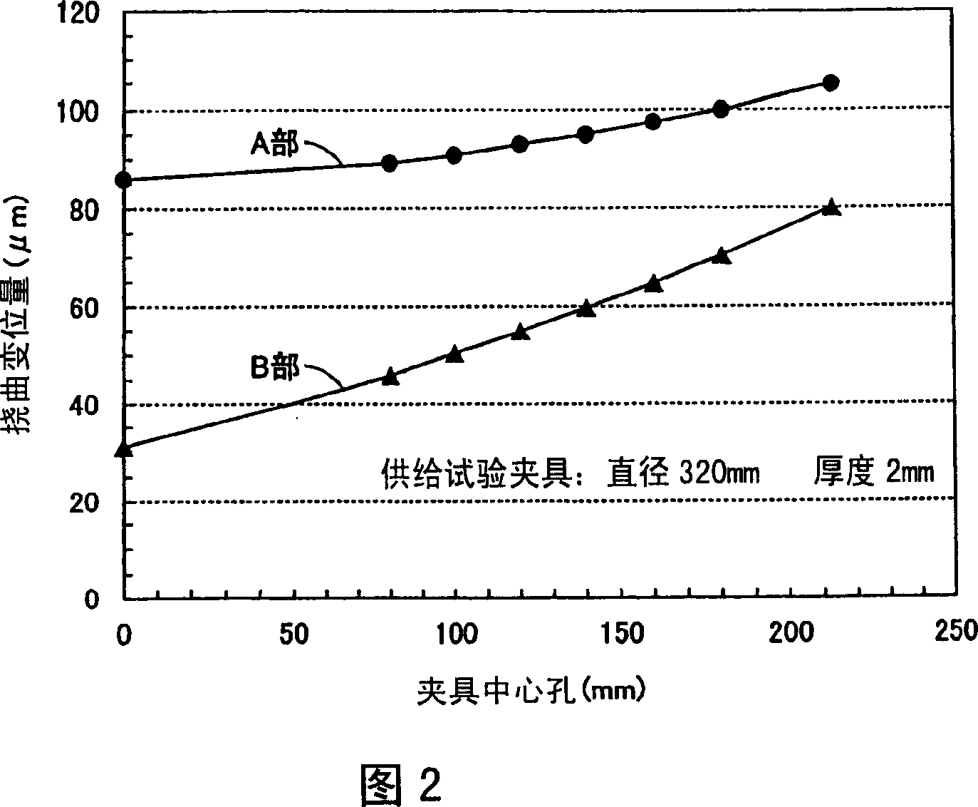
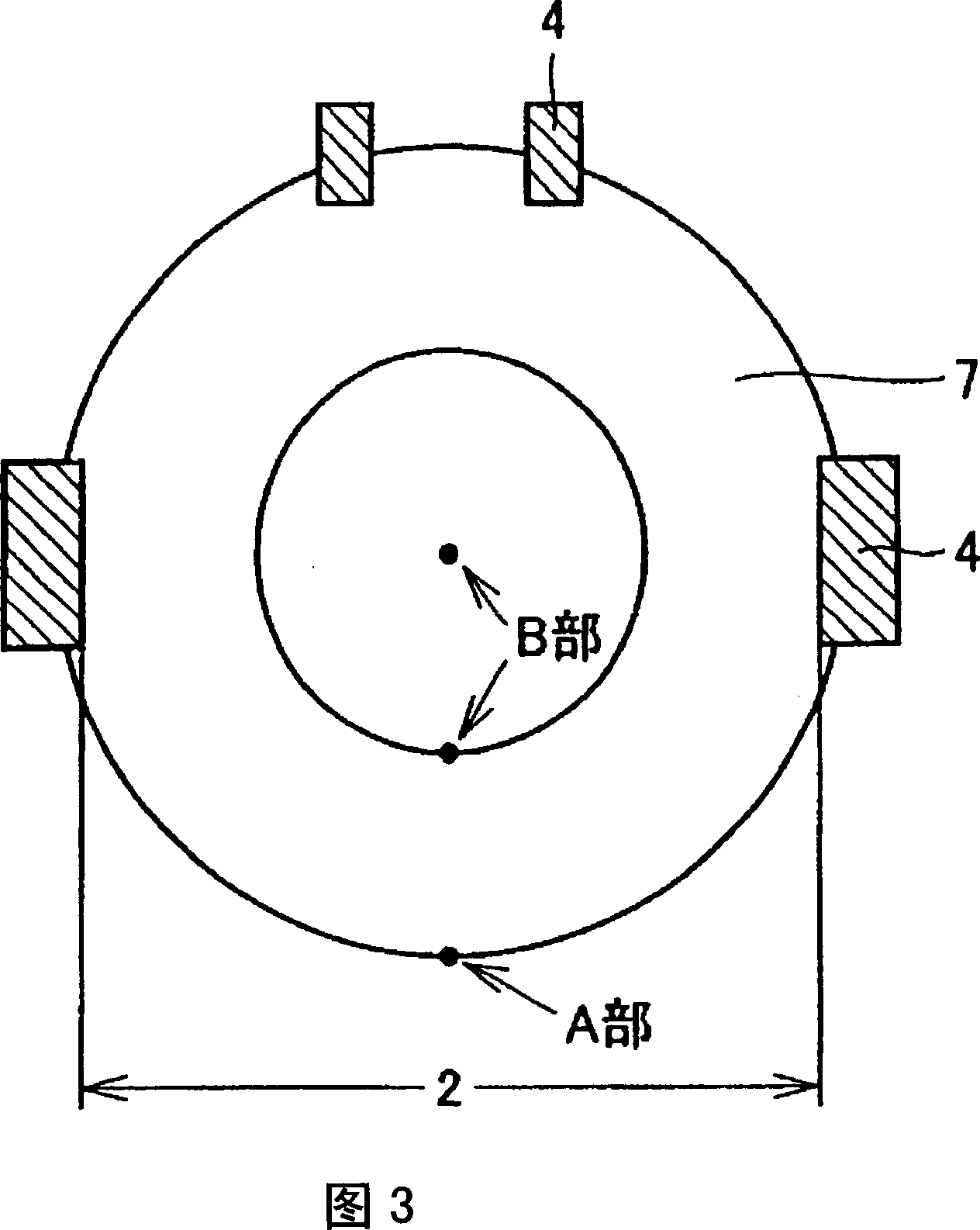

Image

  • Heat treatment jig for silicon semiconductor substrate
  • Heat treatment jig for silicon semiconductor substrate
  • Heat treatment jig for silicon semiconductor substrate

Examples


Embodiment 1

[0080] In order to confirm whether the thickness of the jig is appropriate, as the jig of Invention Example No. 1, three silicon carbide (SiC) circular plate structure heat treatment jigs with a diameter of 319 mm, a thickness of 1.5 mm, and a deflection displacement It is 40 μm to 60 μm, and the surface roughness is 1.5 μm to 1.7 μm.

[0081] Similarly, as the jig of Comparative Example No. 1, three SiC heat treatment jigs with a disc structure of 319 mm in diameter, 0.9 mm in thickness, 50 μm to 80 μm in deflection displacement, and surface roughness 1.4 μm to 1.7 μm.

[0082] A silicon substrate with a diameter of 300mm is loaded on these heat treatment jigs, and the temperature is raised from 600°C to 1000°C at a rate of 5°C / min in an argon atmosphere in a vertical heat treatment furnace at a rate of 3°C / min. Raise the temperature to 1200°C and keep it at 1200°C for one hour, then cool down to 600°C at a rate of 3°C / min. The silicon substrate after heat treatment was obs...

Embodiment 2

[0086] As the jig of Invention Example No. 2, fifty SiC disc-shaped heat treatment jigs with a diameter of 319 mm, a thickness of 2.0 mm, a deflection displacement of 30 μm to 60 μm, and a surface roughness of 1.5 μm~2.0μm.

[0087] The same heat treatment as in Example 1 was performed after mounting the obtained jigs of Invention Example No. 2 on a vertical heat treatment boat at a pitch of 12 mm. The silicon substrate after heat treatment was observed with a magic mirror device for smooth cracks. As a result, most of the silicon substrates had smooth cracks on the outer periphery.

[0088] Next, after mounting the same jigs of Invention Example No. 2 on a vertical heat treatment boat at a pitch of 12 mm, heat treatment was carried out under the same conditions as above, but the heating and cooling rate from 1000°C to 1200°C was changed to 1.5°C / minute. Observation of the silicon substrate after the heat treatment revealed that smooth cracks formed in the outer peripheral ...

Embodiment 3

[0092] Furthermore, jigs of Invention Examples Nos. 4 to 6 described below were produced using the remaining material subjected to the opening processing in the above-mentioned Example 2.

[0093] First, as the jig of Invention Example No. 4, ten heat treatment jigs with a circular plate structure made of SiC with a diameter of 210 mm, a thickness of 1.8 mm, a deflection displacement of 30 μm to 60 μm, and a surface roughness of 2.1 μm ~ 2.3 μm.

[0094] Next, as the jig of Invention Example No. 5, ten heat treatment jigs with a ring structure made of SiC having a diameter of 210 mm, an inner diameter of 205 mm, a thickness of 1.8 mm, a deflection displacement of 30 μm to 60 μm, and a surface The roughness is 2.1 μm to 2.2 μm.

[0095] Furthermore, as the jig of Invention Example No. 6, ten heat treatment jigs with a ring structure made of SiC having a diameter of 210 mm, an inner diameter of 200 mm, a thickness of 1.8 mm, a deflection displacement of 30 μm to 60 μm, and a su...


PUM

PropertyMeasurementUnit
roughnessaaaaaaaaaa
diameteraaaaaaaaaa
roughnessaaaaaaaaaa

Abstract

A heat treatment jig for a semiconductor silicon substrate making contact with a semiconductor silicon substrate to hold the substrate is to be mounted on a heat treatment boat in a vertical heat treatment furnace. The jig has a ring structure or a disc structure, with a thickness of 1.5mm or more but not more than 6.0mm and a flexure displacement quantity of 100mum or less in an area making contact with the semiconductor silicon substrate when mounted on the heat treatment boat. An outer diameter of the jig making contact with the semiconductor silicon substrate to hold the substrate is 65% or more of a diameter of the semiconductor silicon substrate, a surface roughness (Ra value) of a plane making contact with the semiconductor silicon substrate is 1.0mum or more but not more than 100mum. The heat treatment jig effectively reduces slipping, and at the same time, prevents growth suppression of a thermally oxidized film on a substrate rear plane, and eliminates a front plane step, which causes defocusing in a photolithography process in device manufacture. Thus, a high quality of the semiconductor silicon substrate can be maintained and device yield can be remarkably improved.

Description

technical field [0001] The present invention relates to a heat treatment jig used in a heat treatment boat (heat treatment boat) of a vertical heat treatment furnace. In more detail, it relates to a heat treatment jig for a semiconductor silicon substrate, which can reduce the Smooth cracks (slips) generated by crystal defects, and further heat treatment in a high-temperature oxidizing atmosphere can prevent surface steps caused by growth inhibition of thermal oxide films on the back of the held silicon substrate . Background technique [0002] Semiconductor silicon substrates processed in the manufacturing process of LSI devices are manufactured by repeating high-temperature heat treatment in processes such as oxidation, diffusion, and film formation. In the heat treatment of semiconductor silicon substrates, since the vertical heat treatment furnace can reduce the installation space and is suitable for heat treatment of a large number of large-diameter semiconductor silic...

Claims


Application Information

Patent Timeline
Patent Type & Authority Applications(China)
IPC IPC(8): H01L21/22H01L21/31H01L21/324H01L21/68F27D5/00H01L21/673
CPCH01L21/6732H01L21/67306H01L21/67323H01L21/67309F27D5/0037H01L21/67303
Inventor 足立尚志
Owner SUMCO CORP
Learn More