Levenson type phase shift mask and production method therefor
一种相移掩模、掩模的技术,应用在图纹面的照相制版工艺、照相制版工艺曝光装置、半导体/固态器件制造等方向,能够解决剥落、接触面积减小、插入部分分辨率特性降低等问题
- Summary
- Abstract
- Description
- Claims
- Application Information
AI Technical Summary
Problems solved by technology
Method used
Image

Examples
no. 1 example ;
[0051] (first embodiment; type 1)
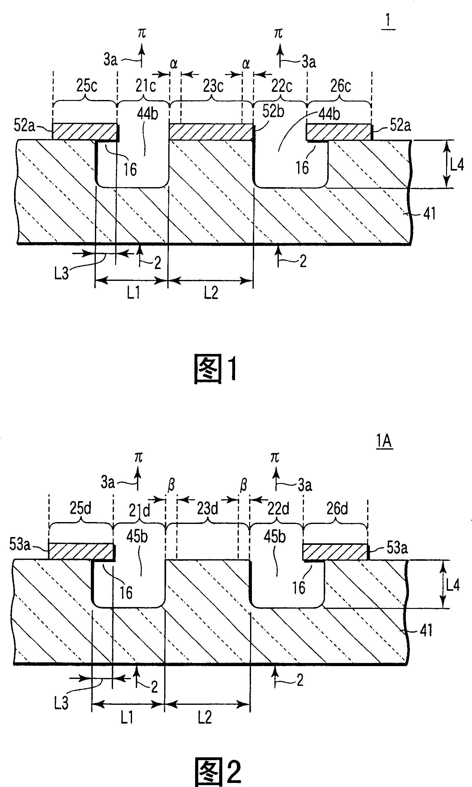
[0052] As shown in FIG. 1, the Levenson type phase shift mask 1 of the first embodiment is a type in which the light shielding portion pattern 23c inserted between adjacent phase shifter openings 21c and 22c from both sides includes a light shielding film pattern 52b, and the light-shielding film pattern 52b has no undercut, and in addition, the light-shielding part pattern 23c is subject to offset correction α. Hereinafter this is referred to as type 1.
[0053] In the mask 1 of type 1, the light-shielding film pattern 52b without the undercut is provided on one side of the excavated part 44b, and the light-shielding film pattern 52a (the light-shielding part pattern 25c) having the undercut 16 is provided on the excavated part 44b. on the other side, and these patterns form phase shifter openings 21c. In the same manner, the phase shifter opening 22c on the other side beyond the light shielding portion pattern 23c is formed by the light ...
no. 2 example
[0055] (second embodiment; type 2)
[0056] As shown in FIG. 2, the mask 1A of the second embodiment is of the type in which the light-shielding portion pattern 23d inserted between adjacent phase shifter openings 21d and 22d from both sides does not have any light-shielding film, and The light shielding portion pattern 23d is subjected to offset correction β. Hereinafter this is referred to as Type 2.
[0057] In the mask 1A of type 2, a light-shielding portion pattern 23d without a light-shielding film is provided on one side of the excavated portion 45b, and a light-shielding film pattern 53a (light-shielding portion pattern 25d ) having an undercut 16 is provided on the other side of the excavated portion 45b. ), and these patterns form phase shifter openings 21d. In the same manner, the phase shifter opening 22d on the other side beyond the light shielding portion pattern 23d is also formed by the light shielding portion pattern 23d without the light shielding film and ...
no. 3 example ;
[0059] (third embodiment; type 3)
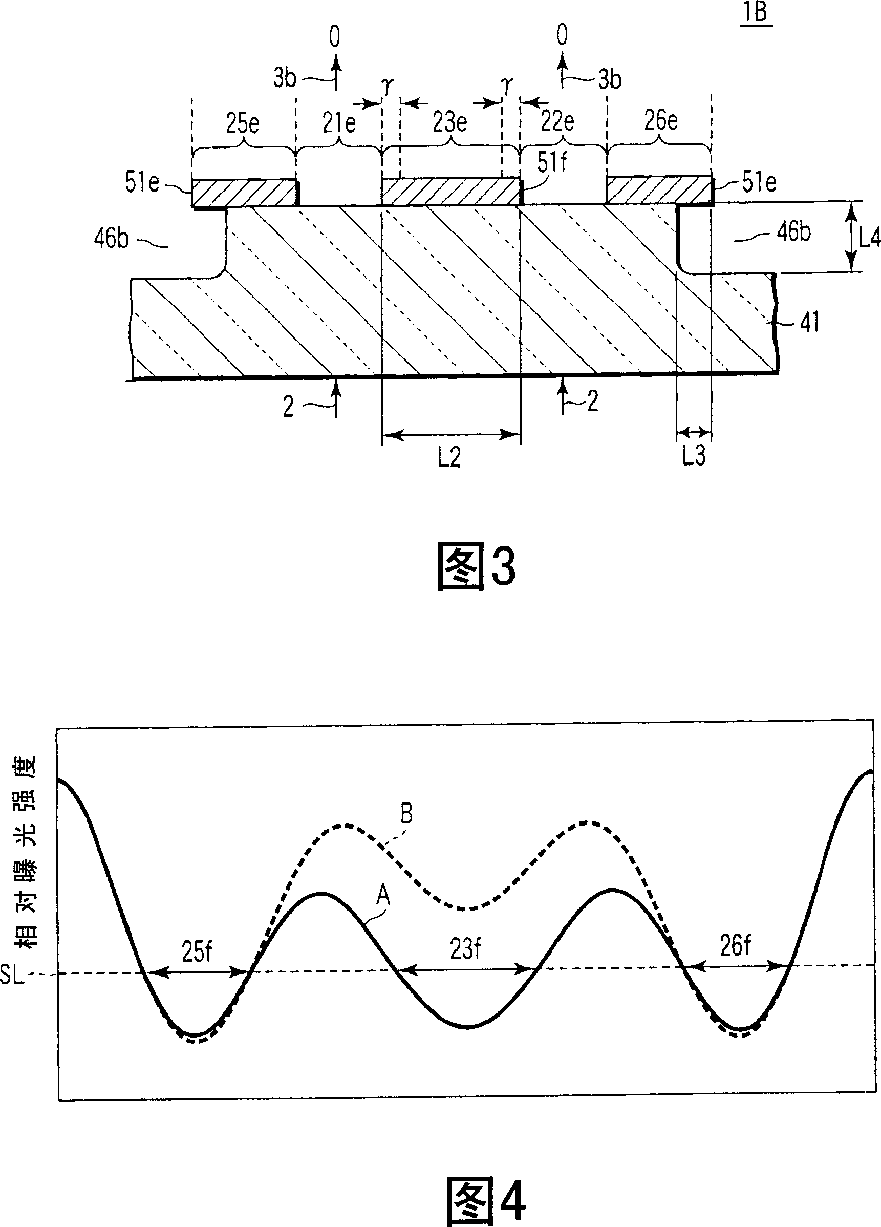
[0060] As shown in FIG. 3, the mask 1B of the third embodiment is of the type in which the light-shielding portion pattern 23e inserted between adjacent non-phase shifter openings 21e and 22e from both sides is subjected to offset correction γ. Hereinafter this is referred to as type 3.
[0061] In the mask 1B of type 3, it is provided not in the excavated portion 46b serving as the phase shifter opening, but in the flat area of the substrate 41 inserted from both sides between the non-phase shifter openings 21e and 22e The light-shielding film pattern 51f, thereby forming the light-shielding portion pattern 23e. According to this mask 1B of type 3, effects of improving resolution characteristics and preventing peeling of the light-shielding film can also be obtained, as in the case of the mask 1A of type 1 described above.
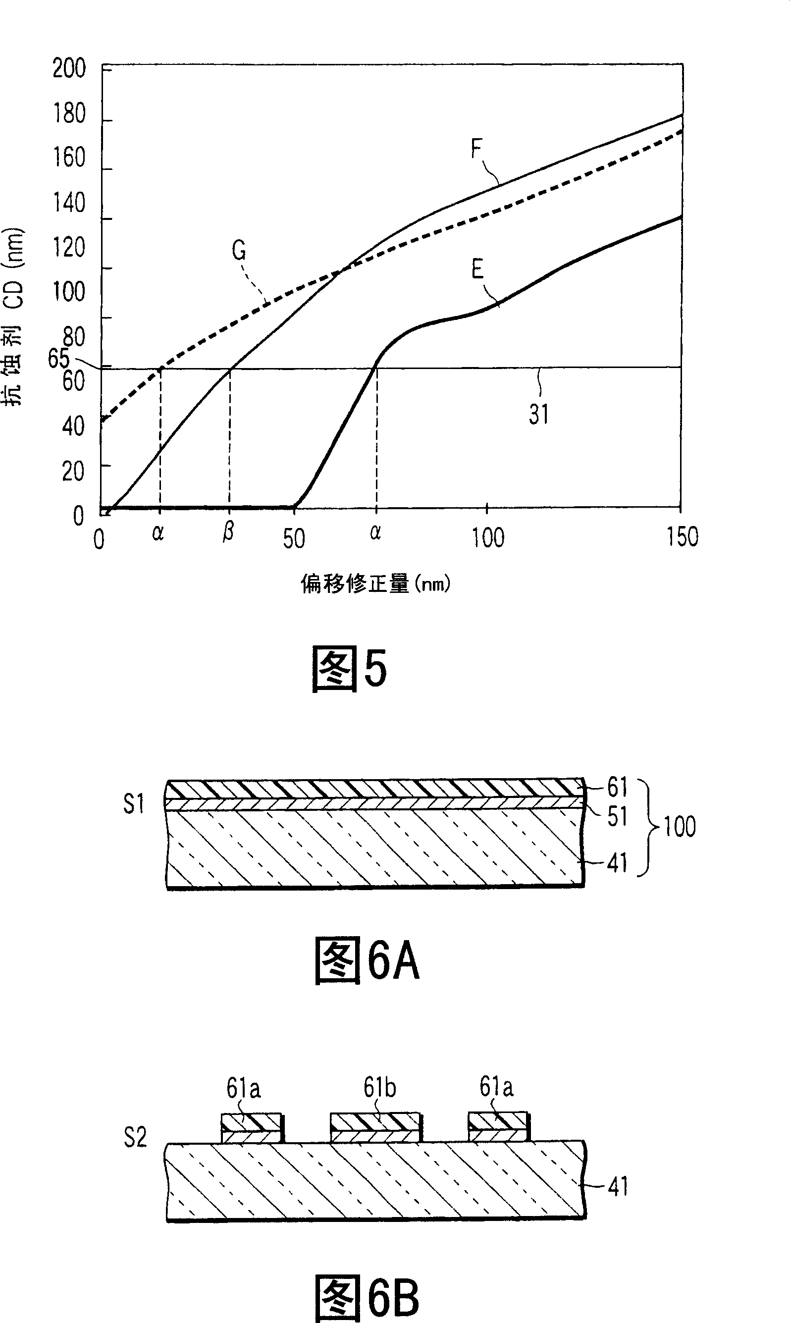
[0062] Next, a simulation of transfer to a semiconductor wafer to obtain an optimum offset correction amount (α, ...
PUM
 Abstract
Description
Claims
Application Information
 - Generate Ideas
- Intellectual Property
- Life Sciences
- Materials
- Tech Scout
- Unparalleled Data Quality
- Higher Quality Content
- 60% Fewer Hallucinations
Browse by: Latest US Patents, China's latest patents, Technical Efficacy Thesaurus, Application Domain, Technology Topic, Popular Technical Reports.
© 2025 PatSnap. All rights reserved.Legal|Privacy policy|Modern Slavery Act Transparency Statement|Sitemap|About US| Contact US: help@patsnap.com