Broadband and wide wave beam microband antenna unit
A technology of microstrip antenna and wide bandwidth, which is applied in the direction of antenna, electrical components, radiation element structure, etc., can solve the problems of narrow beam and bandwidth, achieve mutual compensation, overcome the effect of narrow radiation beam and size reduction
- Summary
- Abstract
- Description
- Claims
- Application Information
AI Technical Summary
Problems solved by technology
Method used
Image
Examples
Embodiment 1
[0025] Embodiment 1: Wide Bandwidth Beam Microstrip Antenna Unit
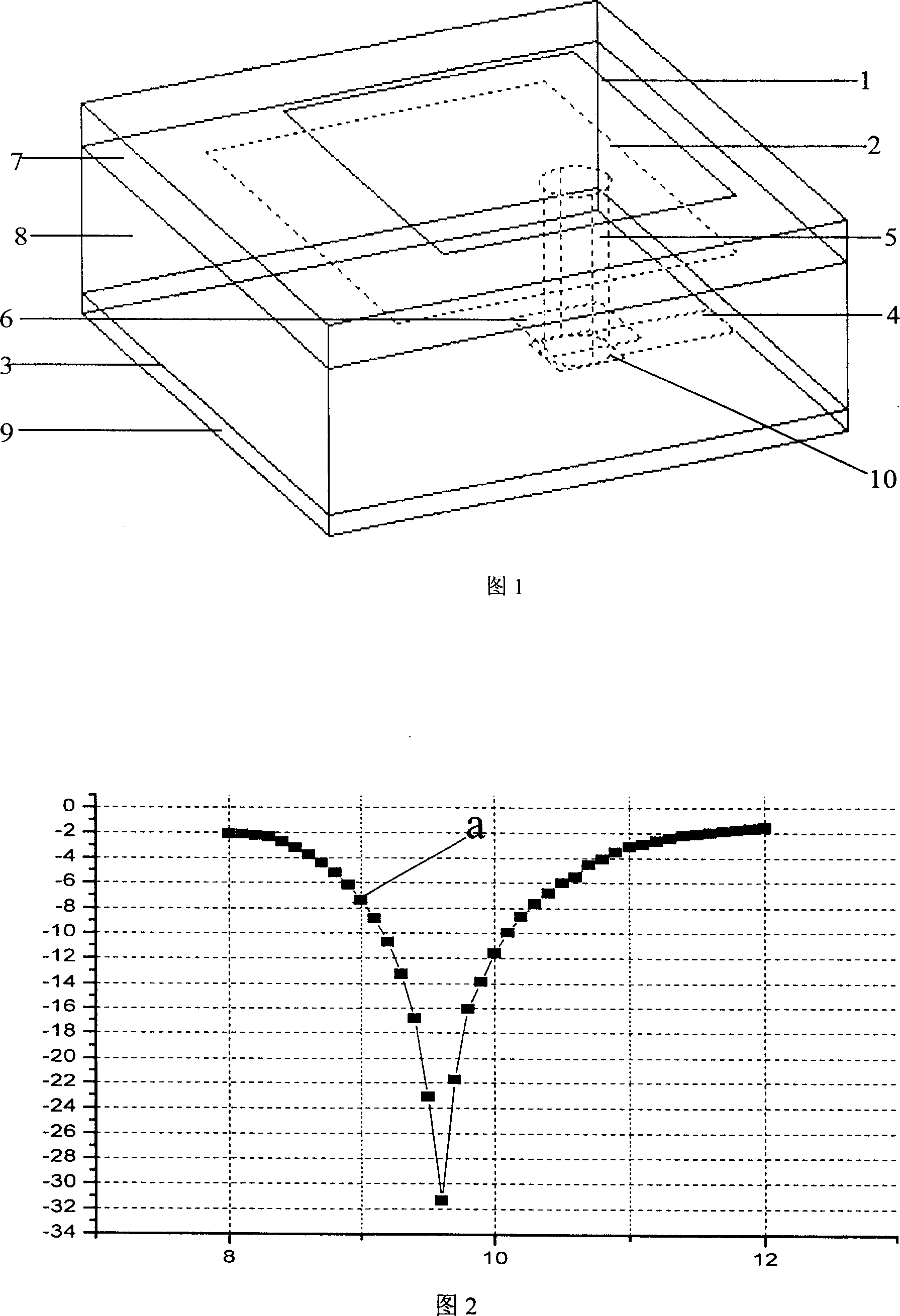
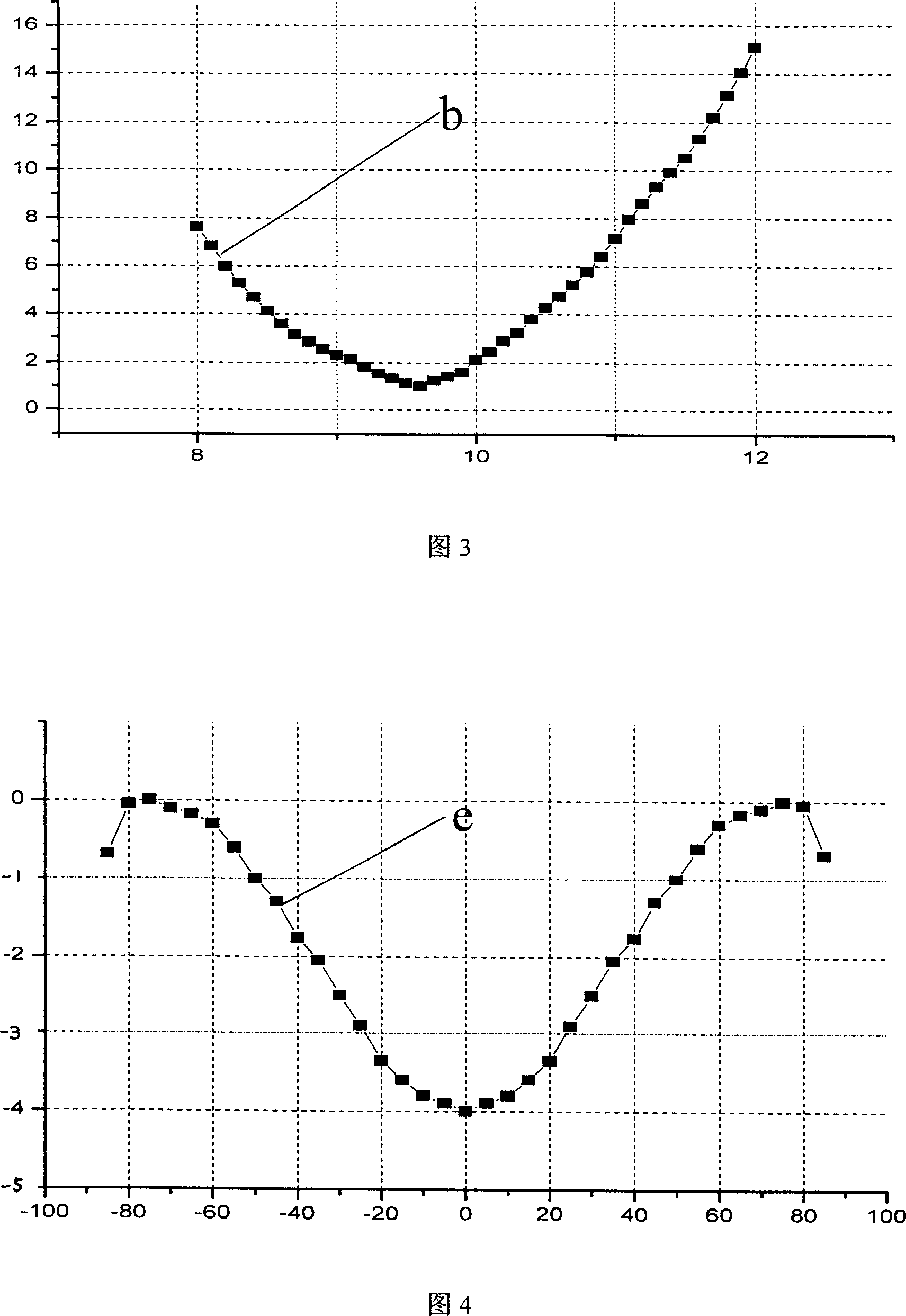
[0026] This embodiment adopts the combination of small hole coupling and multi-layer microstrip technology: three layers of rectangular metal patches with a dielectric constant of 1.07 to 2.2 and a thickness of 0.2mm and 2mm are sandwiched between four layers of rectangular metal patches whose length and width are respectively parallel to each other. The dielectric layer between them; the third layer of metal patch is the ground metal patch 3; the fourth layer of metal patch is used as the microstrip transmission line 4; the length of the long side of the second layer of metal patch 2 is longer than that of the first layer of metal patch The length of the long side of sheet 1 is not more than 1.4 times the length of the long side of the first metal patch 1, the length of the wide side of the second layer of metal patch 2 is longer than the wide side of the first layer of metal patch 1, and No more than 1.3 time...
Embodiment 2
[0045] Embodiment 2: L-band bandwidth beam microstrip antenna unit
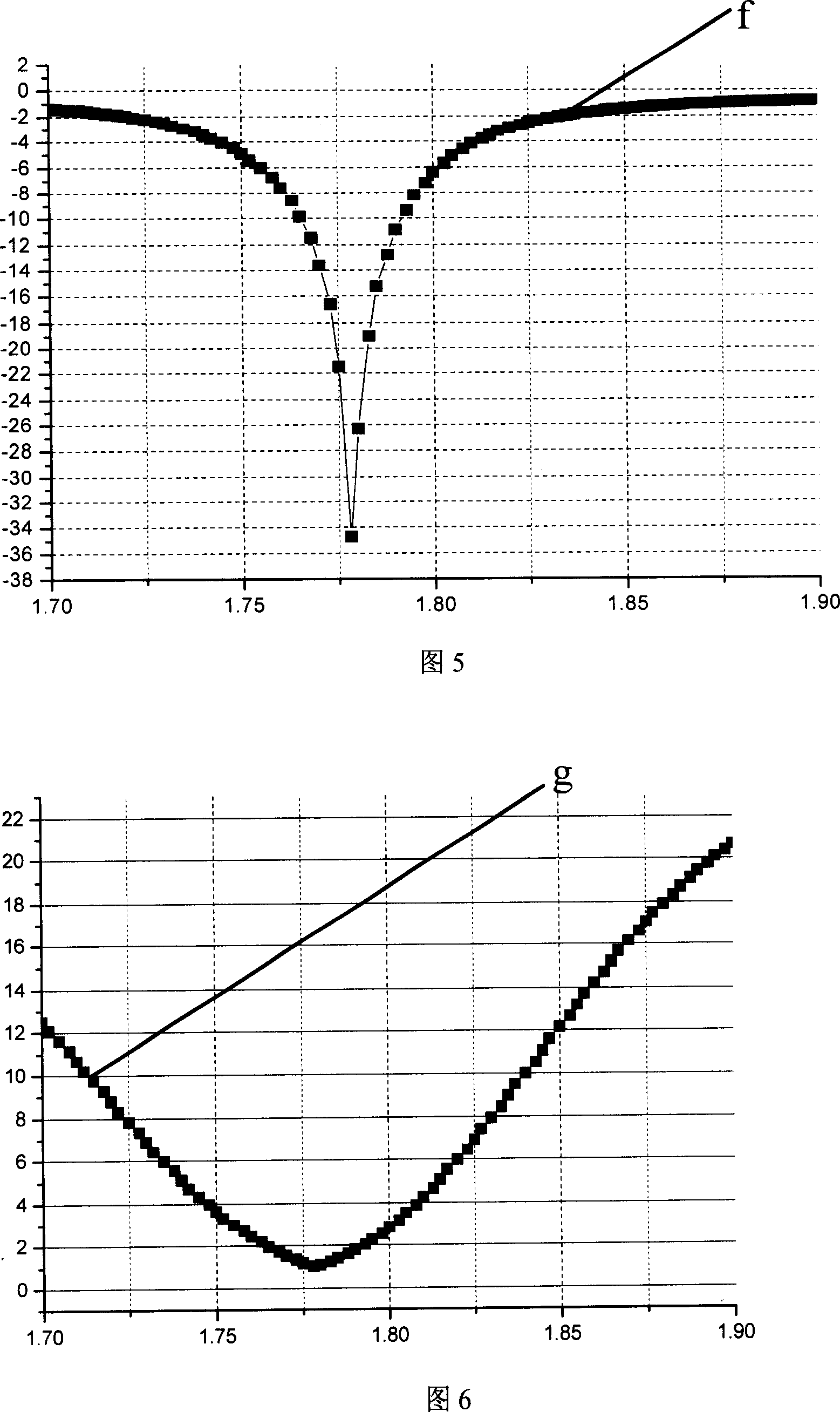
[0046]This embodiment is composed of four layers of rectangular metal patches whose length and width are parallel to each other, and three dielectric layers with a dielectric constant of 1.07 to 2.2 and a thickness between 0.2mm and 2mm are sandwiched between them; the third layer of metal patch is grounded. Metal patch 3; the fourth layer of metal patch is used as a microstrip transmission line 4; the length of the long side of the second layer of metal patch 2 is longer than the long side of the first layer of metal patch 1, and does not exceed the length of the first layer of metal patch 1.4 times the length of the long side of sheet 1, the length of the wide side of the second layer of metal patch 2 is longer than that of the first layer of metal patch 1, and not more than 1.3 times the length of the wide side of the first layer of metal patch 1 ; Take the long side direction of each rectangular entity as...
Embodiment 3
[0065] Example 3: Array Effects
[0066] Four identical antenna units in the above-mentioned embodiment 1 are fabricated together by printing technology, two horizontally and two vertically, forming a 2×2 array. In this array, the antenna units are symmetrical up and down, left and right antennas, the distance between the unit centers along the horizontal direction is 14mm, and the distance along the vertical direction is 13mm. Central location.
[0067] FIG. 5 shows a schematic diagram of the structure of the wide-bandwidth beam microstrip antenna unit in this embodiment after 2×2 array formation, wherein the horizontal axis is the x-axis, and the vertical axis is the y-axis. The input port is drawn from the microstrip transmission line labeled X in Figure 5, and each unit of the array is fed with equal amplitude and same phase.
[0068]In this embodiment, the following effects can be achieved after the wide bandwidth beam microstrip antenna unit is formed into a 2×2 array:...
PUM
 Abstract
Description
Claims
Application Information


