
Methods of forming alpha and beta tantalum films with controlled and new microstructures

A microstructure and thin film technology, applied in the field of tantalum thin films, can solve problems such as unsatisfactory thin films

Inactive Publication Date: 2007-06-20
H C STARCK GMBH +1
View PDF5 Cites 2 Cited by
  • Summary
  • Abstract
  • Description
  • Claims
  • Application Information

AI Technical Summary

Problems solved by technology

Films with this microstructure are less desirable for use in microelectronic devices since Cu can diffuse along the film at grain boundaries

Method used


Image

  • Methods of forming alpha and beta tantalum films with controlled and new microstructures
  • Methods of forming alpha and beta tantalum films with controlled and new microstructures
  • Methods of forming alpha and beta tantalum films with controlled and new microstructures

Examples


Embodiment

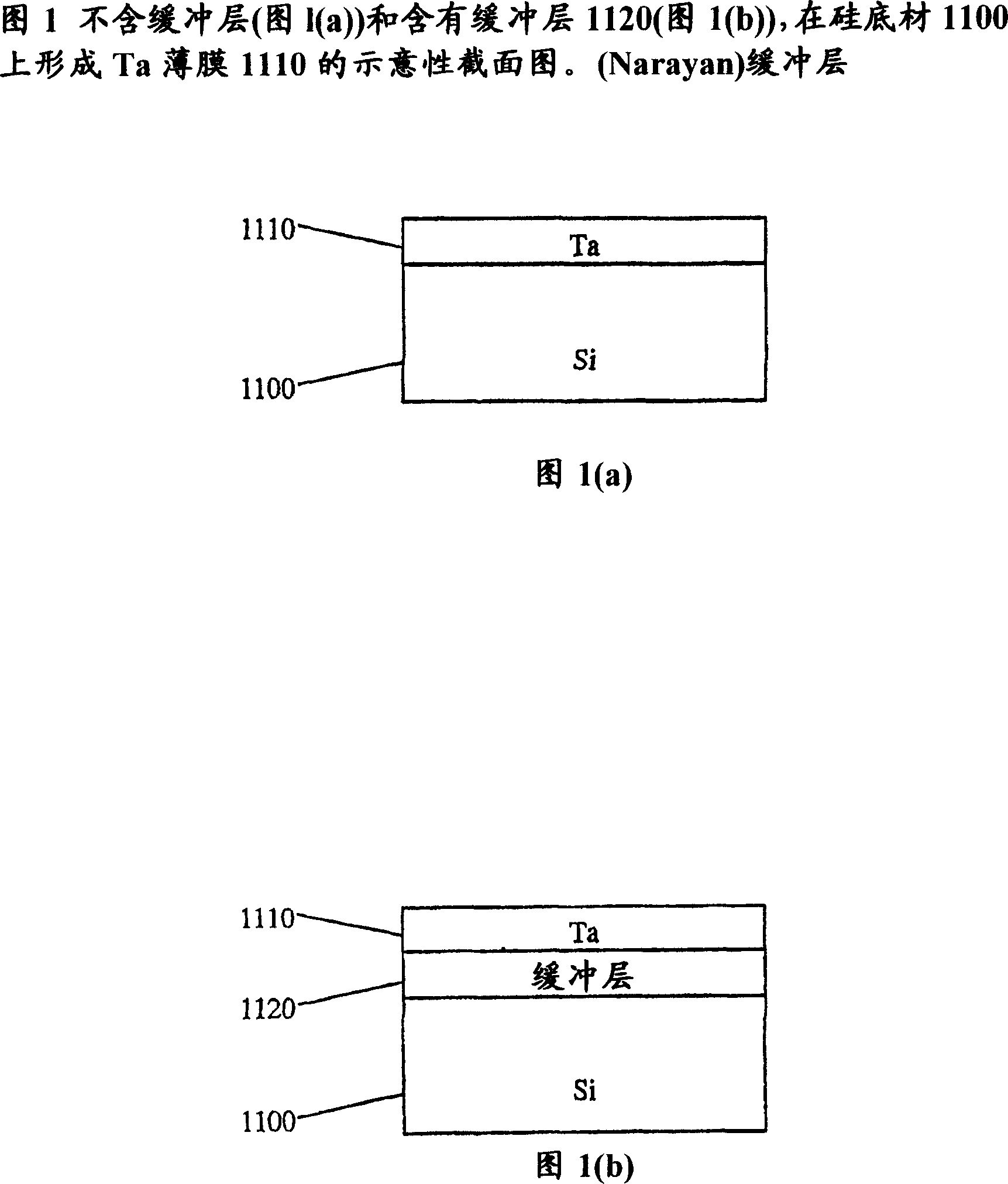
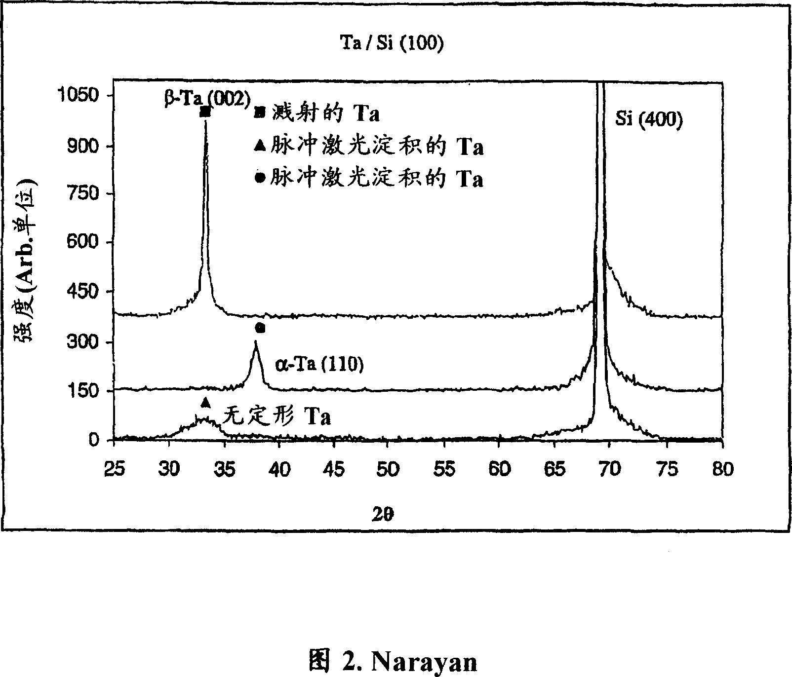
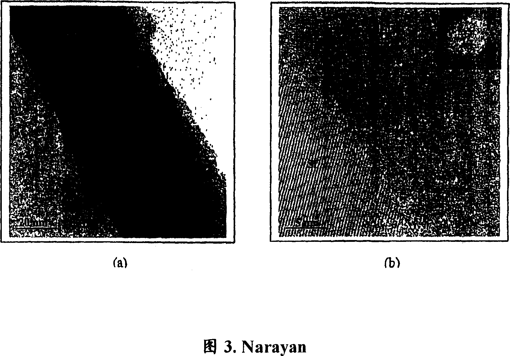
[0052] Scanning Transmission Electron Microscopy Z-contrast images (STEM Z) provide contrast for individual elements based on atomic number (Z2 dependent) differences. Electron Energy Loss Spectroscopy (EELS) analyzes composition by detecting the electronically characteristic energy loss of specific elements. These methods are all powerful tools for the determination of Cu diffusion maps with high precision (0.16 nm spatial resolution), compared to SIMS maps with a resolution of the order of 10 nm. Therefore, HRTEM, STEM-Z contrast images, EELS, atomic structure images, and compositional analyzes were performed on α-Ta thin films with amorphous to single-crystalline microstructures, and the results were compared with large-area SIMS.

[0053]Tantalum (α-Ta) thin films with amorphous to nanocrystalline to polycrystalline to single crystalline microstructures were formed on silicon (Si) substrates with and without buffer layers. Alpha-tantalum (α-Ta) films with grain sizes rang...


PUM


Abstract

Thin tantalum films having novel microstructures are provided. The films have microstructures such as nanocrystalline, single crystal and amorphous. These films provide excellent diffusion barrier properties and are useful in microelectronic devices. Methods of forming the films using pulsed laser deposition (PLD) and molecular beam epitaxy (MBE) deposition methods are also provided, as are microelectronic devices incorporating these films.

Description

field of invention [0001] The present invention relates to tantalum thin films having a novel microstructure that provides improved diffusion resistance. More specifically, the present invention provides single crystalline, nanocrystalline and amorphous tantalum thin films. This film is used in microelectronic applications that require a diffusion barrier between copper interconnects and silicon substrates. Methods of depositing such films on substrates and articles containing tantalum barrier films are also described. Background of the invention [0002] Metallic copper (Cu) has attracted much attention as an interconnect layer in silicon microelectronic devices due to its low resistivity (volume resistivity of 1.67 μΩ-cm) and high resistance to electromigration and stress migration. O. Olowolafe, J. Li, J. W. Mayer: J. Appl. Physics., 68(12), 6207 (1990); S. P. Murarka, Mater. Sci. Eng., R. 19, 87 (1997). However, the diffusion coefficient of Cu in silicon is high (D≈10...

Claims


Application Information

Patent Timeline
Patent Type & Authority Applications(China)
IPC IPC(8): B81C1/00C23C14/16C23C16/06C23C14/54C30B23/00C30B29/02C30B25/00
CPCC23C14/548C23C14/16C23C16/06
Inventor J·纳拉彦P·库马吴荣祯
Owner H C STARCK GMBH
Learn More