Thin film transistor
A thin film transistor, amorphous silicon technology, applied in the direction of transistors, etc., can solve the problems of the thin film transistor 200 not operating normally, the tolerance is insufficient, and the misalignment of the gate 202 and the channel layer 206 is not considered, so as to overcome the errors. Alignment issues, process compatibility, the effect of improved manufacturing yield
- Summary
- Abstract
- Description
- Claims
- Application Information
AI Technical Summary
Problems solved by technology
Method used
Image

Examples
no. 1 example
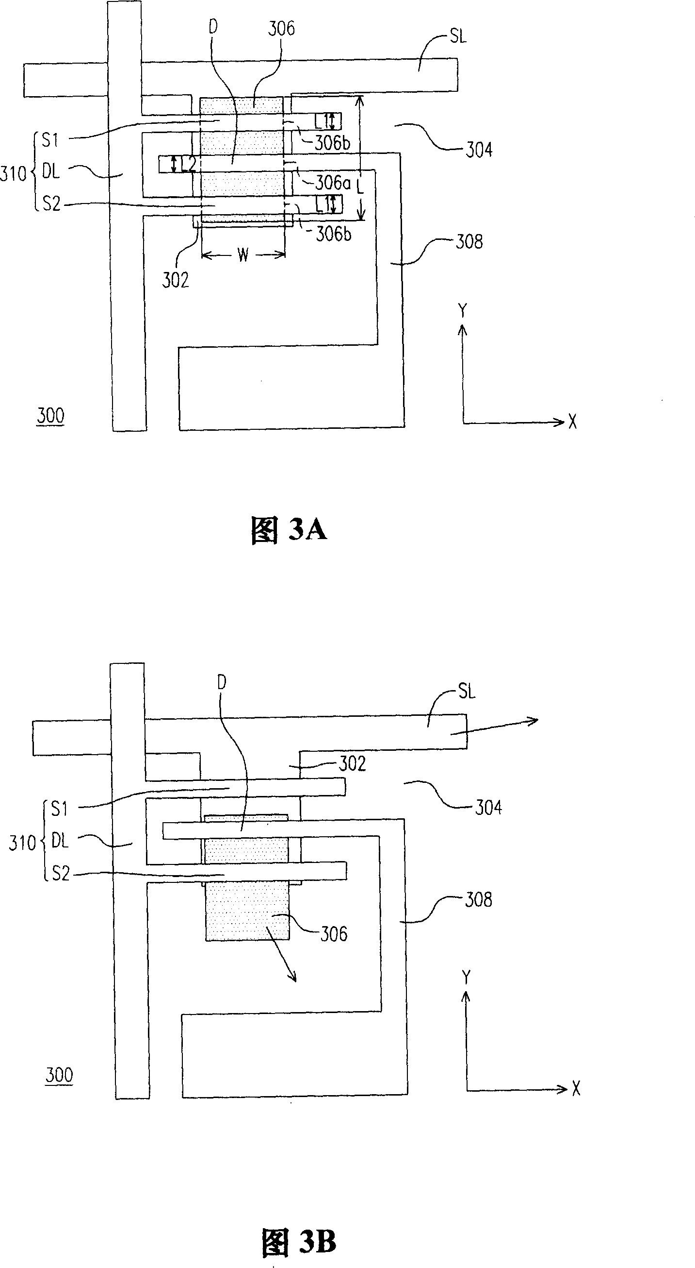
[0051] FIG. 3A is a schematic layout diagram of a thin film transistor according to a first embodiment of the present invention. Please refer to FIG. 3A, the thin film transistor 300 of this embodiment is suitable for being arranged on a flexible substrate (not shown in the figure), and the thin film transistor 300 includes a gate 302, a gate insulating layer 304, a channel layer 306, a first The conductor pattern 308 and the second conductor pattern 310 . Wherein, the gate 302 is disposed on the flexible substrate, and the gate insulation layer 304 is disposed on the flexible substrate to cover the gate 302 . The channel layer 306 is disposed on the gate insulating layer 304 and above the gate 302 . The channel layer 306 has at least one first contact region 306a and a plurality of second contact regions 306b, and the first contact region 306a is located between the second contact regions 306b. In addition, the first conductive pattern 308 is disposed on a portion of the ga...
no. 2 example
[0059] FIG. 4A is a schematic layout diagram of a thin film transistor according to a second embodiment of the present invention. Please refer to FIG. 4A , the thin film transistor 300a of this embodiment is similar to the thin film transistor 300 of the first embodiment, and both belong to a thin film transistor with a dual source structure. The extension direction of the pole S2 and the drain D. In detail, in the thin film transistor 300 a of this embodiment, the extending direction of the source S1 , the source S2 and the drain D is parallel to the extending direction of the data line DL.
[0060] FIG. 4B is a schematic diagram of misalignment of the thin film transistor of the second embodiment. Please refer to FIG. 4B, when misalignment occurs between the gate 302, the channel layer 306, the first conductor pattern 308, and the second conductor pattern 310 due to the expansion and contraction of the flexible substrate, the source S1 and the drain The channel layer 306 b...
no. 3 example
[0062] FIG. 5A is a schematic layout diagram of a thin film transistor according to a third embodiment of the present invention. Please refer to FIG. 5A, the thin film transistor 300b of this embodiment is similar to the thin film transistor 300a of the second embodiment, but the main difference between the two is: the thin film transistor 300b of this embodiment does not have a source S1, only has a source S2 and Data line DL. In detail, in the thin film transistor 300b of this embodiment, the second conductor pattern 310 includes the source S2 and a data line DL connected to the source S2, and the source S2 and the data line DL respectively cover the corresponding first The second contact area 306b.
[0063] In this embodiment, the extending direction of the source S2 and the drain D is parallel to the extending direction of the data line DL. In addition, the distribution position and quantity of the second contact region 306b in this embodiment are no longer determined by...
PUM
 Abstract
Description
Claims
Application Information