MEMS component

a technology of components and components, applied in the field of components, can solve problems such as detrimental effect on the function of components, and achieve the effects of high specific resistance, high electrical insulation effect, and easy variabl

Active Publication Date: 2018-06-19
ROBERT BOSCH GMBH
View PDF9 Cites 0 Cited by
  • Summary
  • Abstract
  • Description
  • Claims
  • Application Information

AI Technical Summary

Benefits of technology

[0008]The mechanical layer properties of a layer based on silicon-carbonitride (Si1-x-yCxNy) depend on their material composition, i.e., on the proportions of the individual material components silicon Si, carbon C and nitrogen N, but also on possible further material components. Accordingly, certain layer properties such as the mechanical tension are easily variable and adaptable to the respective function of the self-supporting structural element.
[0009]In addition, it is advantageous that silicon carbonitride-based layers are easily able to be produced with the aid of standard deposition methods such as in an LPCVD (low pressure chemical vapor deposition) method at temperatures in the range from 700-900° C. As an alternative, such layers are also able to be deposited in a PECVD (plasma enhanced chemical vapor deposition) process at 300-800° C. In this context, silane SiH4, methane CH4 or ammonia NH3 may be used as starting gases. Standard methods such as DRIE (deep reactive ion etching) using SF6 are also able to be used for the structuring of layers based on silicon carbonitride.
[0011]Layers having this composition exhibit slight tensile tensioning and high breaking tension which therefore makes them mechanically very robust as a whole.
[0012]The tensioning state of silicon carbonitridoboride layers Si1-x-y-zCxNyBz with x, y, z>1% is particularly easy to adjust. A layer composition having a 35 at % Si content, 35 at % C content, 20 at % N content and 10 at % B content is advantageous.

Problems solved by technology

In all cases, leakage currents between the electrode and the abutting carrier material of the structural element have a detrimental effect on the component function.

Method used


Image

  • MEMS component
  • MEMS component
  • MEMS component

Examples


Embodiment Construction

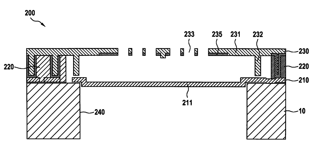
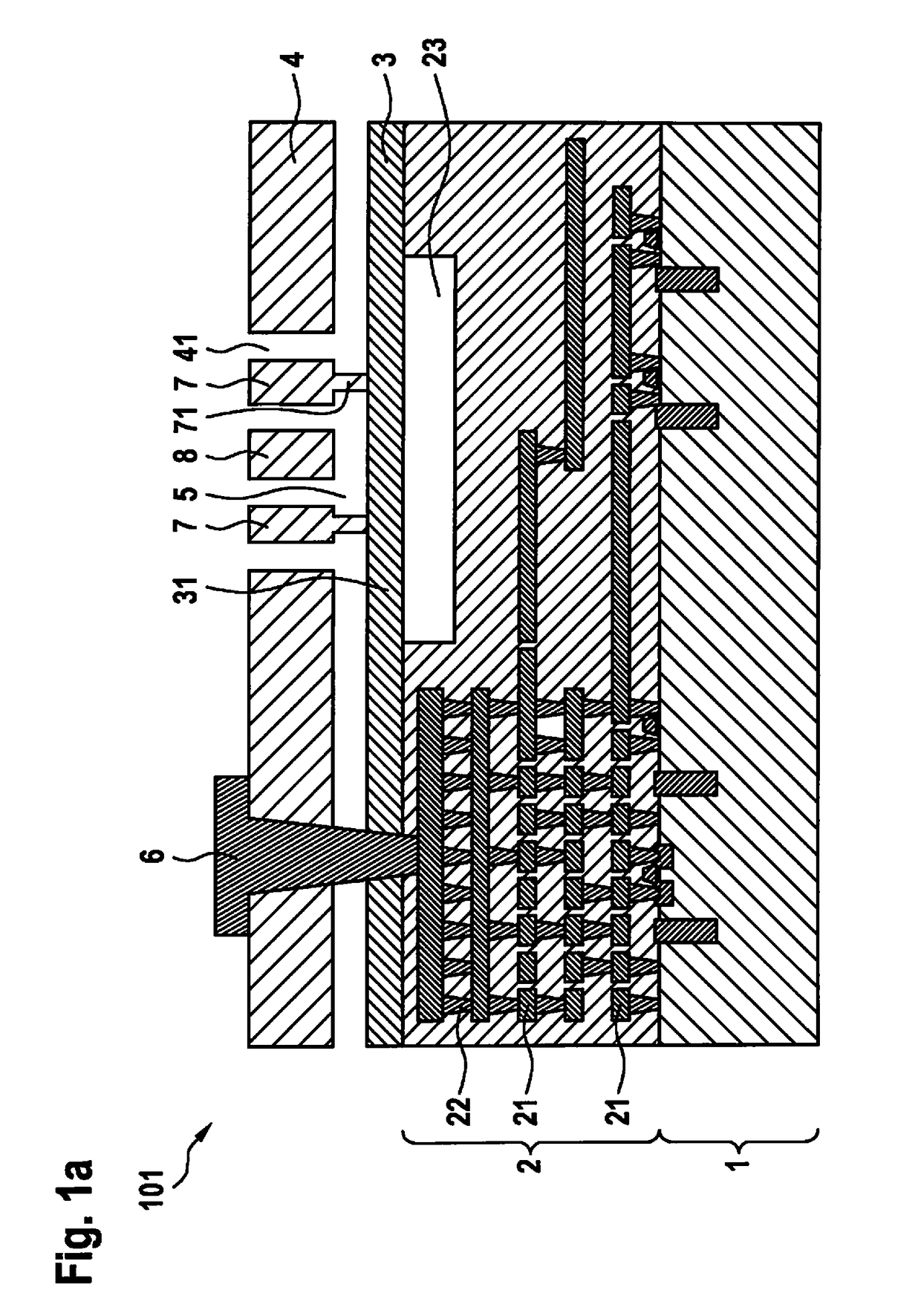
[0021]The layer structure of the two components 101 and 102 shown in FIGS. 1a and 1b is based on a respective CMOS substrate 1 into which circuit functionalities (not shown here in detail) are integrated. They are connected to each other via a back-end stack 2 having multiple wiring planes 21 and through contacts 22 between wiring planes 21 and are electrically contactable. In the exemplary embodiment shown, the electrical contacting takes place by way of a through contact 6, which extends from the front side of the component to the uppermost wiring plane of back-end stack 2.

[0022]Situated on back-end stack 2 is a relatively thin layer 3 based on silicon carbonitride in which a self-supporting pressure diaphragm 31 is developed. It spans a cavity 23 in back-end stack 2. The layer structure of components 101 and 102 furthermore includes a relatively thick functional layer 4, which is structured in the region above pressure diaphragm 31. Functional layer 4 was provided with through ho...


PUM


Abstract

A layer material which is particularly suitable for the realization of self-supporting structural elements having an electrode in the layer structure of a MEMS component. The self-supporting structural element is at least partially made up of a silicon carbonitride (Si1-x-yCxNy)-based layer.

Description

BACKGROUND INFORMATION[0001]In general terms, the present invention relates to MEMS components in whose layer structure at least one self-supporting structural element having at least one electrode is realized.[0002]The self-supporting structural element may be a micromechanical component which has its own sensor or actuator functionality, for instance the diaphragm of a pressure sensor, a microphone or an amplifier. However, the self-supporting structural element may also serve simply as a carrier for a sensor functionality, for instance in the case of a flow-rate sensor having heating resistors which are present on a diaphragm for the thermal decoupling. Accordingly, the electrode of the self-supporting structural element may be utilized as a capacitor electrode for acquiring measuring signals or for the excitation of vibrations or also simply for the electrical contacting of an electrical resistor or some other circuit component. In all cases, leakage currents between the electro...

Claims


Application Information

Patent Timeline
Patent Type & Authority Patents(United States)
IPC IPC(8): H01L29/84B81B3/00
CPCB81B3/0086B81B2201/01B81B2201/0228B81B2201/0257B81B2201/0264B81B2203/0127B81B2203/0136B81C1/00801
Inventor SCHELLING, CHRISTOPHSTEIN, BENEDIKTSTUMBER, MICHAEL
Owner ROBERT BOSCH GMBH
Why Eureka
Try Eureka