Selective deposition of metallic films

a technology of metallic film and selective deposition, which is applied in the direction of semiconductor devices, semiconductor/solid-state device details, electrical apparatus, etc., can solve the problems of sharp decrease in the mean time to failure, small devices, and difficulty in implementing a selective metal cap, and achieve enhanced atomic layer deposition and chemical vapor deposition.

Active Publication Date: 2018-07-03
ASM IP HLDG BV
View PDF185 Cites 210 Cited by
  • Summary
  • Abstract
  • Description
  • Claims
  • Application Information

AI Technical Summary

Benefits of technology

[0010]In some aspects processes are presented herein for selectively depositing a film on a substrate comprising a first metallic surface and a second surface comprising silicon. In some embodiments the processes may comprise passivating a reaction chamber in which a selective deposition process is to be performed, subjecting the substrate to a first surface treatment process comprising exposing the substrate to a plasma, subsequent to the first surface treatment process, performing one or more selective deposition cycles in the reaction chamber, each cycle comprising contacting the substrate with a first precursor comprising silicon or boron to selectively form a layer of first material comprising Si or B on the first metallic surface relative to the second surface comprising silicon, and converting the first material on the first metallic surface to a second metallic material by exposing the first material to a second precursor comprising metal. In some embodiments the second metallic material is deposited on the first metallic surface of the substrate relative to the second surface comprising silicon with a selectivity of greater than about 50%.
[0011]In some embodiments the first metallic surface comprises copper. In some embodiments the f...

Problems solved by technology

Meeting the ever increasing electromigration (EM) requirement in copper interconnects is becoming more difficult as Moore's law progresses, resulting in smaller devices.
As line dimensions shrink, critical void size for EM failure is also reduced, causing a sharp decrease in mean time to failure....

Method used


Image

  • Selective deposition of metallic films
  • Selective deposition of metallic films
  • Selective deposition of metallic films

Examples


examples

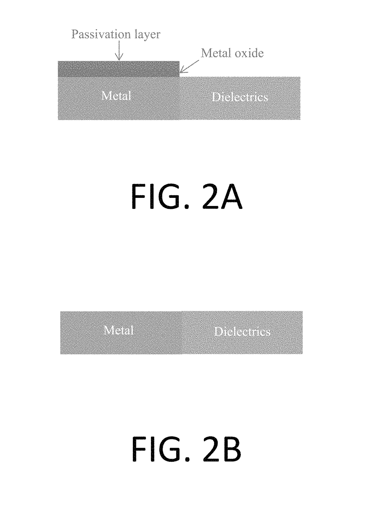
[0232]Sample substrates having a first metallic surface comprising Cu and a second dielectric surface comprising a low-k dielectric material having a dielectric constant of 3.0 were provided and the first Cu surface was passivated by depositing an organic layer thereon, having a thickness of about 1 nm to 2 nm. A native copper oxide layer was also present between the Cu surface and the organic layer, having a thickness of about 1 nm. Substrates comprising only a Co surface, along with a native cobalt oxide surface layer, were also provided to act as controls.

[0233]The sample substrates comprising a first Cu surface and a second dielectric surface, along with the control substrates comprising a Co surface were subjected to various first surface treatment processes in order to investigate the effects of such processes on a subsequently performed selective deposition process for depositing W on the first surface of the sample substrate relative to the second surface, as described herei...


PUM


Abstract

Metallic layers can be selectively deposited on one surface of a substrate relative to a second surface of the substrate. In some embodiments, the metallic layers are selectively deposited on a first metallic surface relative to a second surface comprising silicon. In some embodiments the reaction chamber in which the selective deposition occurs may optionally be passivated prior to carrying out the selective deposition process. In some embodiments selectivity of above about 50% or even about 90% is achieved.

Description

CROSS-REFERENCE TO RELATED APPLICATIONS[0001]The present application is a continuation-in-part of U.S. application Ser. No. 15 / 177,198, filed Jun. 8, 2016, and entitled “SELECTIVE DEPOSITION OF METALLIC FILMS,” and U.S. application Ser. No. 15 / 177,195, filed Jun. 8, 2016, and entitled “REACTION CHAMBER PASSIVATION AND SELECTIVE DEPOSITION OF METALLIC FILMS,” and is related to U.S. application Ser. No. 13 / 708,863, filed Dec. 7, 2012, and entitled “SELECTIVE FORMATION OF METALLIC FILMS ON METALLIC SURFACES” which claims priority to U.S. Provisional Application No. 61 / 569,142, filed Dec. 9, 2011, the disclosures of which are hereby incorporated by reference in their entireties.BACKGROUNDField[0002]The present application relates generally to the field of semiconductor fabrication.Description of the Related Art[0003]Integrated circuits are currently manufactured by an elaborate process in which various layers of materials are sequentially constructed in a predetermined arrangement on a ...

Claims


Application Information

Patent Timeline
IPC IPC(8): H01L21/768H01L21/285H01L23/532
CPCH01L21/7685H01L21/28562H01L21/28568H01L23/53238H01L21/76826H01L21/76868H01L21/76823H01L23/53228H01L23/53266H01L21/76883H01L21/3105H01L21/76849H01L21/02068
Inventor CHEN, SHANGWATARAI, TOSHIHARUONUMA, TAKAHIROISHIKAWA, DAINAMBA, KUNITOSHI
Owner ASM IP HLDG BV
Why Eureka
Try Eureka