
Spatial positioning of photon emitters in a plasmonic illumination device

a plasmonic illumination and spatial positioning technology, applied in semiconductor devices, lighting and heating apparatus, instruments, etc., can solve the problems of scattering losses, further losses, and absorption losses, and achieve the effect of increasing the tapering of the antenna elements, increasing the magnetic and magneto-electric response, and increasing the tapering

Active Publication Date: 2018-07-10
LUMILEDS
View PDF7 Cites 4 Cited by
  • Summary
  • Abstract
  • Description
  • Claims
  • Application Information

AI Technical Summary

Benefits of technology

The present device allows for precise control over the distance between the antenna array and the photon emitting layer using a thick layer in which the antenna elements are embedded. This distance is important for achieving a self-aligned three-dimensional distribution of the wavelength converting material that matches the distribution of maximum field enhancement, without the need for complex patterning methods. The technical effect of this is that it greatly increases the availability of the illumination device.

Problems solved by technology

This means that blue light will also be scattered back into the diode which leads to absorption losses in the LED.
This leads to further losses as only a portion of the light escapes through the output surface of the light emitting device.
However, to be able to control the emission direction, a photonic band gap material needs to be made from materials having a high refractive index contrast, high aspect ratio holes or pillars must be patterned and formed, the size control is very strict and the material must be luminescent which will incur scattering losses.
Furthermore, a photonic band gap material is only really effective in the plane perpendicular to the surface of the material, i.e. in a direction parallel to the holes or pillars.
Accordingly, the suggested approaches for increasing the emission efficiency of a light emitting device suffer from inherent drawbacks which are hard to overcome.

Method used


Image

  • Spatial positioning of photon emitters in a plasmonic illumination device
  • Spatial positioning of photon emitters in a plasmonic illumination device
  • Spatial positioning of photon emitters in a plasmonic illumination device

Examples


Embodiment Construction

[0048]The present invention will now be described more fully hereinafter with reference to the accompanying drawings, in which exemplary embodiments of the invention are shown. This invention may, however, be embodied in many different forms and should not be construed as limited to the embodiments set forth herein; rather, these embodiments are provided for thoroughness and completeness, and fully convey the scope of the invention to the skilled person. Like reference characters refer to like elements throughout.

[0049]In the present detailed description, various embodiments of the illumination device according to the present invention are mainly discussed with reference to an illumination device with a photon emitting layer comprising wavelength converting particles. It should be noted that this by no means limits the scope of the present invention which is equally applicable to other types of photon emitters which may be comprised in the illumination device.

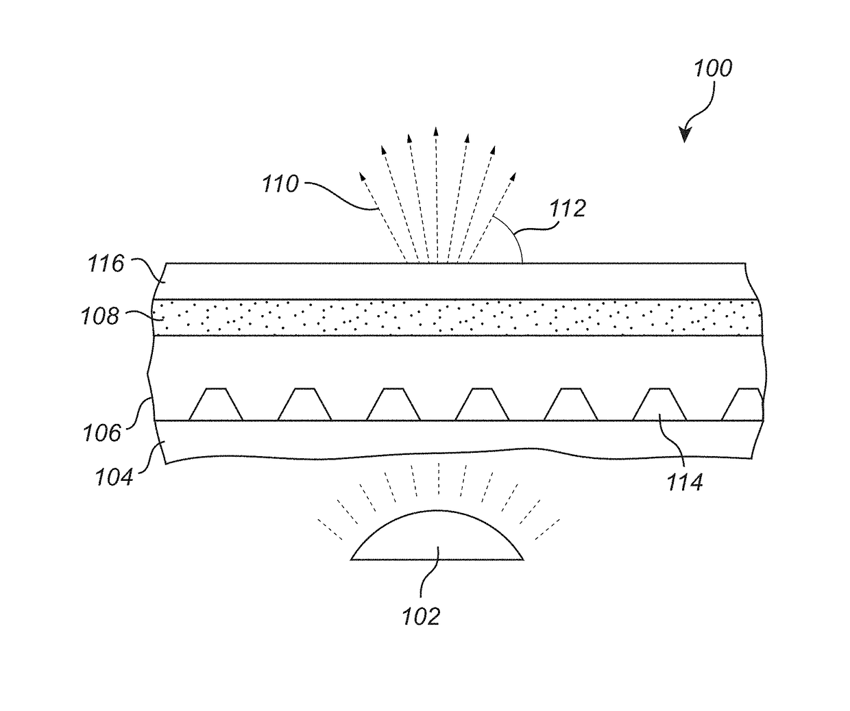
[0050]FIG. 1 is a schem...


PUM

PropertyMeasurementUnit
refractive indexaaaaaaaaaa
distanceaaaaaaaaaa

Abstract

There is provided an illumination device (100) comprising: a substrate (104); an optically transmissive first layer (106) arranged on the substrate; a photon emitting layer (108), arranged on the optically transmissive first layer and comprising a photon emitting material configured to receive energy from an energy source and to emit light having a predetermined wavelength; a periodic plasmonic antenna array, arranged on the substrate and embedded within the first layer, and comprising a plurality of individual antenna elements (114) arranged in an antenna array plane, the plasmonic antenna array being configured to support a first lattice resonance at the predetermined wavelength, arising from coupling of localized surface plasmon resonances in the individual antenna elements to photonic modes supported by the system comprising the plasmonic antenna array and the photon emitting layer, wherein the plasmonic antenna array is configured to comprise plasmon resonance modes such that light emitted from the plasmonic antenna array has an anisotropic angle distribution; and wherein the photon emitting layer is arranged at a distance from the antenna array plane corresponding to a location of maximum field enhancement for light out-coupling resulting from the plasmonic-photonic lattice resonances.

Description

CROSS-REFERENCE TO RELATED APPLICATIONS[0001]The present application is a § 371 application of International Application No. PCT / EP2015 / 061191 filed on May 21, 2015 and entitled “SPATIAL POSITIONING OF PHOTON EMITTERS IN A PLASMONIC ILLUMINATION DEVICE,” which claims the benefit of European Patent Application No. 14170048.4, filed May 27, 2014. PCT / EP2015 / 061191 and EP 14170048.4 are incorporated herein.FIELD OF THE INVENTION[0002]The present invention relates to a plasmonic illumination device. In particular, the present invention relates to optimized spatial positioning of emitters in a plasmonic illumination device, and to a method for manufacturing such a device.BACKGROUND OF THE INVENTION[0003]For light emitting diodes (LEDs) for use in lighting applications, it is desirable to provide essentially white light having a color temperature approximately comparable to that produced by incandescent lighting.[0004]White light from LEDs is commonly provided by using a pn-diode emitting...

Claims


Application Information

Patent Timeline
Patent Type & Authority Patents(United States)
IPC IPC(8): G02F1/03H01L33/50F21V9/30G02F1/29F21K9/64H01L33/58G02B5/00
CPCG02B5/008F21K9/64F21V9/30H01L33/507H01L33/58G02F1/29H01L33/508G02F2203/10F21K9/20H01L33/50F21Y2115/10
Inventor VERSCHUUREN, MARCUS ANTONIUSLOZANO BARBERO, GABRIEL SEBASTIANGOMEZ RIVAS, JAIME
Owner LUMILEDS
Learn More