
Image capturing device and inspection apparatus and inspection method

a technology of image capture and inspection apparatus, which is applied in the direction of optically investigating flaws/contamination, instruments, polarisation-affecting properties, etc., can solve the problems of reducing the production yield of semiconductor elements, reducing inspection accuracy, and prolonging inspection tim

Active Publication Date: 2018-07-31
NUFLARE TECH INC
View PDF37 Cites 2 Cited by
  • Summary
  • Abstract
  • Description
  • Claims
  • Application Information

AI Technical Summary

Benefits of technology

This configuration enables high-accuracy inspection with minimal light degradation, allowing for the detection of fine defects in mask patterns without the need for a half mirror, thereby improving inspection efficiency and accuracy.

Problems solved by technology

A defect of a circuit pattern formed on of a mask or template can be cited as a large factor that reduces a production yield of the semiconductor element.
The difference, for example, can be caused by short defects or open defects.
A shortage of the light quantity causes degradation of inspection accuracy and lengthening of inspection time.

Method used


Image

  • Image capturing device and inspection apparatus and inspection method
  • Image capturing device and inspection apparatus and inspection method
  • Image capturing device and inspection apparatus and inspection method

Examples


Embodiment Construction

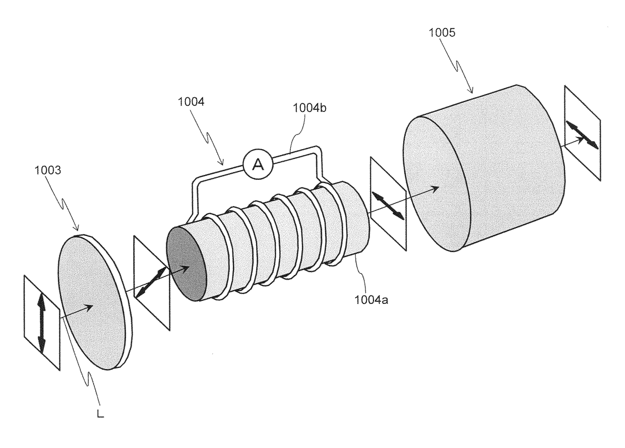
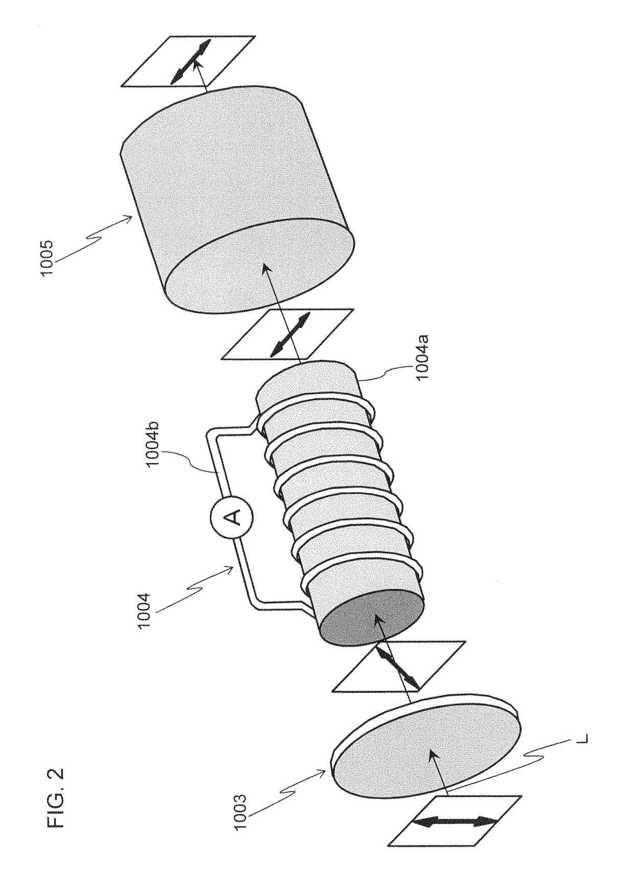
[0049]FIG. 1 illustrates an example of a configuration of an image capturing device according to the present embodiment. The image capturing device includes an illumination optical system OP1 that illuminates a mask 1006, a sensor 1007 that captures an image of a pattern of the mask 1006, and an imaging optical system OP2 that images the light reflected from the mask 1006 onto the sensor 1007.

[0050]The illumination optical system OP1 includes a light source 1001, a beam shaping optical system 1008, a polarization beamsplitter 1002, a half-wavelength plate 1003, a Faraday rotator 1004, and an objective lens 1005. The beam shaping optical system 1008 includes an expander lens that expands a beam, an integrator lens that increases the uniformity of the light to the surface, and a relay lens in which a magnification is set such that a mask surface is illuminated with the beam at a desired size. On the other hand, the imaging optical system OP2 includes the objective lens 1005, the Farad...


PUM

PropertyMeasurementUnit
angleaaaaaaaaaa
angleaaaaaaaaaa
angleaaaaaaaaaa

Abstract

An image capturing device comprising, a light source configured to emit light having a predetermined wavelength, a polarization beamsplitter configured to receive the light from the light source, a Faraday rotator configured to rotate a polarization plane of the light via the polarization beamsplitter by changing the intensity of the magnetic field, an objective lens configured to illuminate an inspection target with the light transmitted through the Faraday rotator and a sensor configured to capture an optical image of the inspection target by causing the light reflected by the inspection target to be incident through the objective lens, the Faraday rotator, and the polarization beamsplitter.

Description

CROSS-REFERENCE TO THE RELATED APPLICATION[0001]The entire disclosure of the Japanese Patent Application No. 2013-175093, filed on Aug. 26, 2013 including specification, claims, drawings, and summary, on which the Convention priority of the present application is based, are incorporated herein in its entirety.FIELD OF THE INVENTION[0002]The present invention relates to an Image Capturing Device and an Inspection Apparatus and Inspection Method.BACKGROUND[0003]Recently, with increasing integration degree of a semiconductor device, dimensions of individual element become finer, and widths of wiring and gate constituting each element also become finer.[0004]A process of transferring an original plate (a mask or a reticle, hereinafter collectively referred to as a mask) to a photosensitive resin to fabricate a wafer is fundamental to production of a semiconductor integrated circuit. The semiconductor integrated circuit is produced by repeating the fundamental process.[0005]An exposure a...

Claims


Application Information

Patent Timeline
Patent Type & Authority Patents(United States)
IPC IPC(8): H04N7/18G01N21/95G01N21/88G01N21/21
CPCG01N21/9501G01N21/21G01N21/8806G01N2201/06113G01N2021/8848
Inventor OGAWA, RIKI
Owner NUFLARE TECH INC
Learn More