Unlock instant, AI-driven research and patent intelligence for your innovation.

Fabricating method of a semiconductor structure with an epitaxial layer

a technology of semiconductor structure and epitaxial layer, which is applied in the direction of semiconductor devices, electrical equipment, basic electric elements, etc., can solve the problems of epitaxial strain, increase the complexity of processing and manufacturing ics, and the size of the device feature is becoming smaller

Active Publication Date: 2018-07-31
UNITED MICROELECTRONICS CORP
View PDF6 Cites 5 Cited by
  • Summary
  • Abstract
  • Description
  • Claims
  • Application Information

AI Technical Summary

Benefits of technology

The present invention provides a method for fabricating a semiconductor structure with different channel strains in a dense region and an isolated region. By using a three-layer material system and etching techniques, the method allows for the formation of both recesses and an epitaxial layer to restore the strain to the structure. This method provides greater flexibility and precision in creating semiconductor structures with different strains and can improve the performance and reliability of semiconductor devices.

Problems solved by technology

With the development of integrated circuits technology, device feature size is becoming smaller, and low electron and hole mobility in bulk silicon material has become the bottleneck of enhancing device performance.
For example, as an epitaxial layer such as SiGe has a different lattice constant from Si, there will be a lattice mismatch between a SiGe substrate and epitaxial Si grown thereon, and such a lattice mismatch will induce strain in an epitaxial Si layer.
These criteria have increased the complexity of processing and manufacturing ICs.

Method used


Image

  • Fabricating method of a semiconductor structure with an epitaxial layer
  • Fabricating method of a semiconductor structure with an epitaxial layer
  • Fabricating method of a semiconductor structure with an epitaxial layer

Examples


Embodiment Construction

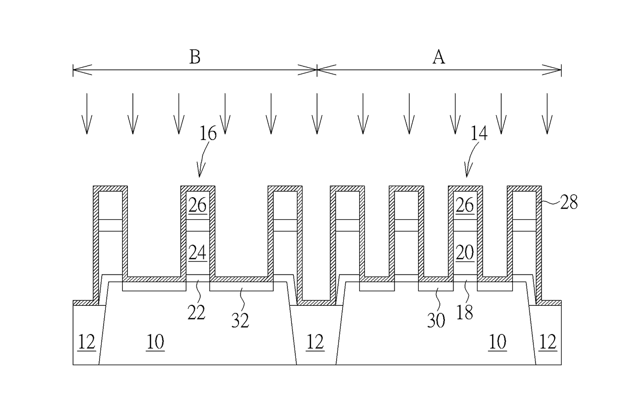
[0020]FIG. 1 to FIG. 12 depict a fabricating method of a semiconductor structure with an epitaxial layer according to a preferred embodiment of the present invention.

[0021]As shown in FIG. 1, a substrate 10 is provided. The semiconductor substrate 10 of the present invention is a bulk silicon substrate, a germanium substrate, a gallium arsenide substrate, a silicon germanium substrate, an indium phosphide substrate, a gallium nitride substrate, a silicon carbide substrate, or a silicon on insulator (SOI) substrate. The substrate 10 may be a planar substrate or fins. The substrate 10 is divided into a dense region A and an isolated region B. Shallow trench isolations 12 are disposed in the substrate 10 to define active regions. The dense region A may be a core region which has a higher element density, and the isolated region B may be an Input / Output (I / O) region which has a lower element density. At least a first gate structure 14 is disposed within the dense region A, and at least ...


PUM


Abstract

A fabricating method of a semiconductor structure includes providing a substrate divided into a dense region and an isolated region, wherein a first gate structure is disposed within the dense region, and a second gate structure is disposed within the isolated region. Then, a first material layer is formed to cover the first gate structure, the second gate structure and the substrate. Later, a second material layer is formed to cover the first material layer. After that, the second material layer within the dense region is entirely removed. Subsequently, a third material layer is formed to cover the isolated region and the dense region. Next, the substrate is etched to forma first recess at two sides of the first gate structure, and a second recess at two sides of the second gate structure. Finally, an epitaxial layer is formed to fill the first recess and the second recess.

Description

BACKGROUND OF THE INVENTION1. Field of the Invention[0001]The present invention relates a fabricating method of a semiconductor structure with an epitaxial layer; and more particularly to a fabricating method of a semiconductor structure having an epitaxial layer farther from a gate structure within an isolated region and nearer to a gate structure within a core region.2. Description of the Prior Art[0002]With the development of integrated circuits technology, device feature size is becoming smaller, and low electron and hole mobility in bulk silicon material has become the bottleneck of enhancing device performance. Strained silicon is formed by epitaxially growing silicon on materials that have a different lattice constant from silicon. Because strained silicon can effectively improve carrier mobility, it has become a candidate substrate material for semiconductor technology nodes of the next generation. For example, as an epitaxial layer such as SiGe has a different lattice const...

Claims


Application Information

Patent Timeline
Patent Type & Authority Patents(United States)
IPC IPC(8): H01L21/8234H01L29/78
CPCH01L21/823418H01L21/823468H01L29/7848H01L21/823437H01L29/66545H01L29/6656H01L29/66636H01L21/823425H01L21/823431H01L21/823821H01L21/845H01L29/66795H01L29/785
Inventor HSU, TE-CHANGCHEN, CHUN-CHIAWANG, YAO-JHAN
Owner UNITED MICROELECTRONICS CORP
Features
  • R&D
  • Intellectual Property
  • Life Sciences
  • Materials
  • Tech Scout
  • Unparalleled Data Quality
  • Higher Quality Content
  • 60% Fewer Hallucinations
Learn More