Unlock instant, AI-driven research and patent intelligence for your innovation.

Semiconductor storage device and method for writing of the same

a storage device and semiconductor technology, applied in the field of semiconductor storage devices and a method for writing of the same, can solve the problems of not necessarily true that the writing is efficiently conducted to all of the memory cells, and the threshold of the memory cells to which data have been written will vary, so as to improve the uniformity of writing and improve the writing efficiency

Active Publication Date: 2018-08-14
DENSO CORP
View PDF10 Cites 0 Cited by
  • Summary
  • Abstract
  • Description
  • Claims
  • Application Information

AI Technical Summary

Benefits of technology

This patent is about a new method for writing to a semiconductor storage device. The method improves the efficiency and consistency of writing to each memory cell. The structure of the device is designed to optimize the writing process. Overall, this method improves the speed and reliability of writing to the semiconductor storage device.

Problems solved by technology

Thus, if the writing is executed under the same condition to all of the memory cells, it is not necessarily true that the writing is efficiently conducted to all of the memory cells.
In such a case, since the state of writing is not uniform, there is a possibility that variations in thresholds of the memory cells to which data have been written will arise.

Method used


Image

  • Semiconductor storage device and method for writing of the same
  • Semiconductor storage device and method for writing of the same
  • Semiconductor storage device and method for writing of the same

Examples


first embodiment

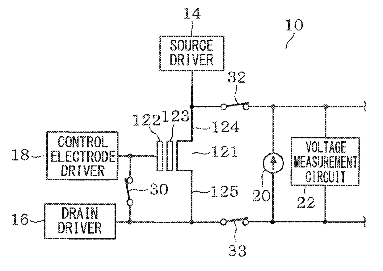
[0027]As shown in FIG. 1, a semiconductor storage device 10 according to the present embodiment is, for example, a p-channel flash memory, and has a memory cell 121. The memory cell 121 has a control electrode 122, a floating electrode 123, a source 124 and a drain 125. Writing to the memory cell 121 is implemented as electrons are injected to the floating electrode 123.

[0028]The semiconductor storage device 10 includes a source driver 14 and a drain driver 16. The source driver 14 is connected to the source 124, and applies a predetermined voltage to the source 124. The drain driver 16 is connected to the drain 125, and applies a predetermined voltage to the drain 125. The semiconductor storage device 10 includes a control electrode driver 18. The control electrode driver 18 is connected to the control electrode 122, and applies a predetermined voltage to the control electrode 122.

[0029]A switch 30 is provided between the control electrode 122 and the drain 125, and is configured t...

second embodiment

[0038]Next, a second embodiment will be described. Hereinafter, only the differences from the first embodiment will be described. The structure of a semiconductor storage device 10 of the second embodiment is the same as the structure of the first embodiment.

[0039]As shown in FIG. 3, in a writing processing of the second embodiment, firstly, the switches 30, 32 and 33 are turned on (B1). Next, a predetermined current is caused to flow to the memory cell 121 from the current source 20 (B2). That is, a voltage is applied between the control electrode 122 connected to the drain 125 and the source 124 so that the predetermined current flows in the memory cell 121. Next, a first potential difference (La, voltage, voltage difference) generated between the source 124 and the drain 125 is measured by the voltage measurement circuit 22 (B3). Since the control electrode 122 and the drain 125 are in the connected state, the first potential difference (voltage) is a threshold voltage of the mem...

third embodiment

[0051]Next, a third embodiment will be described. Hereinafter, only the differences from the first embodiment will be described. As shown in FIG. 5, the third embodiment is different from the first embodiment as having a reference memory cell 121a and a storage memory cell 131.

[0052]As shown in FIG. 5, a semiconductor storage device 10 has a reference memory cell 121a and a storage memory cell 131. The semiconductor storage device 10 includes a source driver 141 that is connected to a source 124a of the reference memory cell 121a, and applies a predetermined voltage to the source 124a. The semiconductor storage device 10 includes a drain driver 161 that is connected to a drain 125a, and applies a predetermined voltage to the drain 125a. Also, the semiconductor storage device 10 includes a control electrode driver 181 that is connected to a control electrode 122a, and applies a predetermined voltage to the control electrode 122a.

[0053]A switch 30 is provided between the control elec...


PUM


Abstract

A semiconductor storage device includes a memory cell, a switch, a source driver, a drain driver, a voltage measurement circuit and a control electrode driver. The memory cell has a control electrode, a floating electrode, a source and a drain. In a writing to the memory cell, the voltage measurement circuit measures a voltage generated between the control electrode and the source when the switch is in an on state connecting the control electrode and the drain and a predetermined current flows from the current source to the memory cell, and the control electrode driver applies to the control electrode a voltage that is controlled based on the voltage measured by the voltage measurement circuit.

Description

CROSS REFERENCE TO RELATED APPLICATIONS[0001]This application is a U.S. national stage of International Patent Application No. PCT / JP2016 / 072463 filed on Aug. 1, 2016 and is based on Japanese Patent Application No. 2015-155081 filed on Aug. 5, 2015, the disclosures of which are incorporated herein by reference.TECHNICAL FIELD[0002]The present disclosure relates to a semiconductor storage device and a method for writing of the same.BACKGROUND ART[0003]For example, in a conventional writing to a p-channel flash memory cell, an application voltage to the memory cell had a fixed value.PRIOR ART LITERATUREPatent Literature[0004]Patent Literature 1 JP2004-55004ANon-Patent Literature[0005]Non-patent Literature 1: Joe Brewer, Manzur Gill, “Nonvolatile Memory Technologies with Emphasis on Flash: A Comprehensive Guide to Understanding and Using Flash Memory Devices”, Wiley-IEEE PressSUMMARY OF INVENTION[0006]Suitable writing conditions are likely to be different between respective memory cell...

Claims


Application Information

Patent Timeline
Patent Type & Authority Patents(United States)
IPC IPC(8): G11C11/34G11C11/404G11C11/4074G11C7/10G11C16/28
CPCG11C11/404G11C16/28G11C11/4074G11C7/1096G11C16/10G11C16/3454G11C2013/0076
Inventor KAI, YOSHIHIDE
Owner DENSO CORP