3D stacked multilayer semiconductor memory using doped select transistor channel

a semiconductor memory and select transistor technology, applied in the direction of semiconductor devices, basic electric elements, electrical equipment, etc., can solve the problems disadvantages of gate oxide injection, and achieve the effect of deterioration of reading latency

Active Publication Date: 2018-10-02
ASM IP HLDG BV
View PDF1603 Cites 333 Cited by
  • Summary
  • Abstract
  • Description
  • Claims
  • Application Information

AI Technical Summary

Benefits of technology

[0008]According to some embodiments, a suitable threshold voltage can be provided to a select transistor without deterioration of reading latency, and also proper isolation can be provided for selecting a memory transistor in a 3D stacked multilayer semiconductor memory.

Problems solved by technology

In stacking of multiple semiconductors such as those in the above examples, one issue to be worked on when using a select transistor is how to perform doping in a channel region of a select transistor because a doping concentration of the select transistor channel has to be different from that of a channel of a memory transistor.
Another issue to be worked on when using a select transistor is how to establish isolation of the select transistor from the memory transistor.
Injecting an electrical charge to the gate oxide involves a disadvantage of deterioration in reading latency.

Method used


Image

  • 3D stacked multilayer semiconductor memory using doped select transistor channel
  • 3D stacked multilayer semiconductor memory using doped select transistor channel
  • 3D stacked multilayer semiconductor memory using doped select transistor channel

Examples


example 1

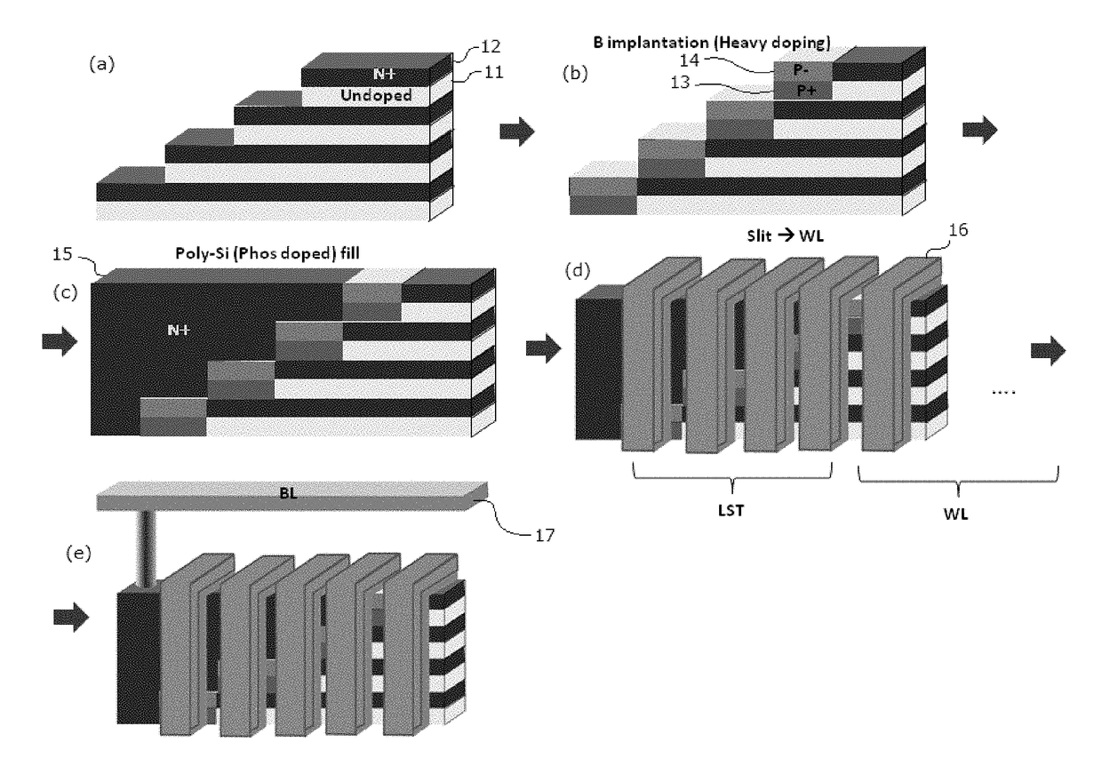
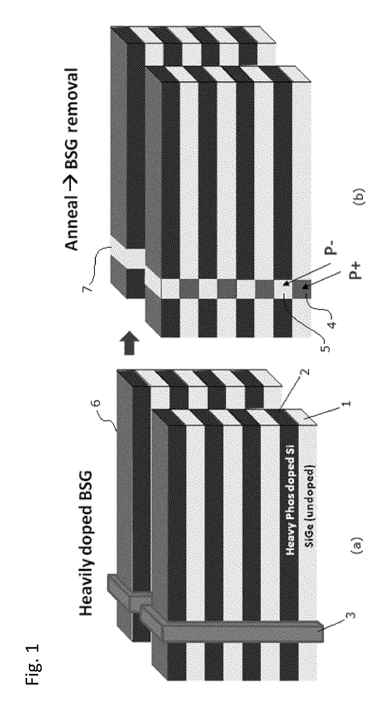
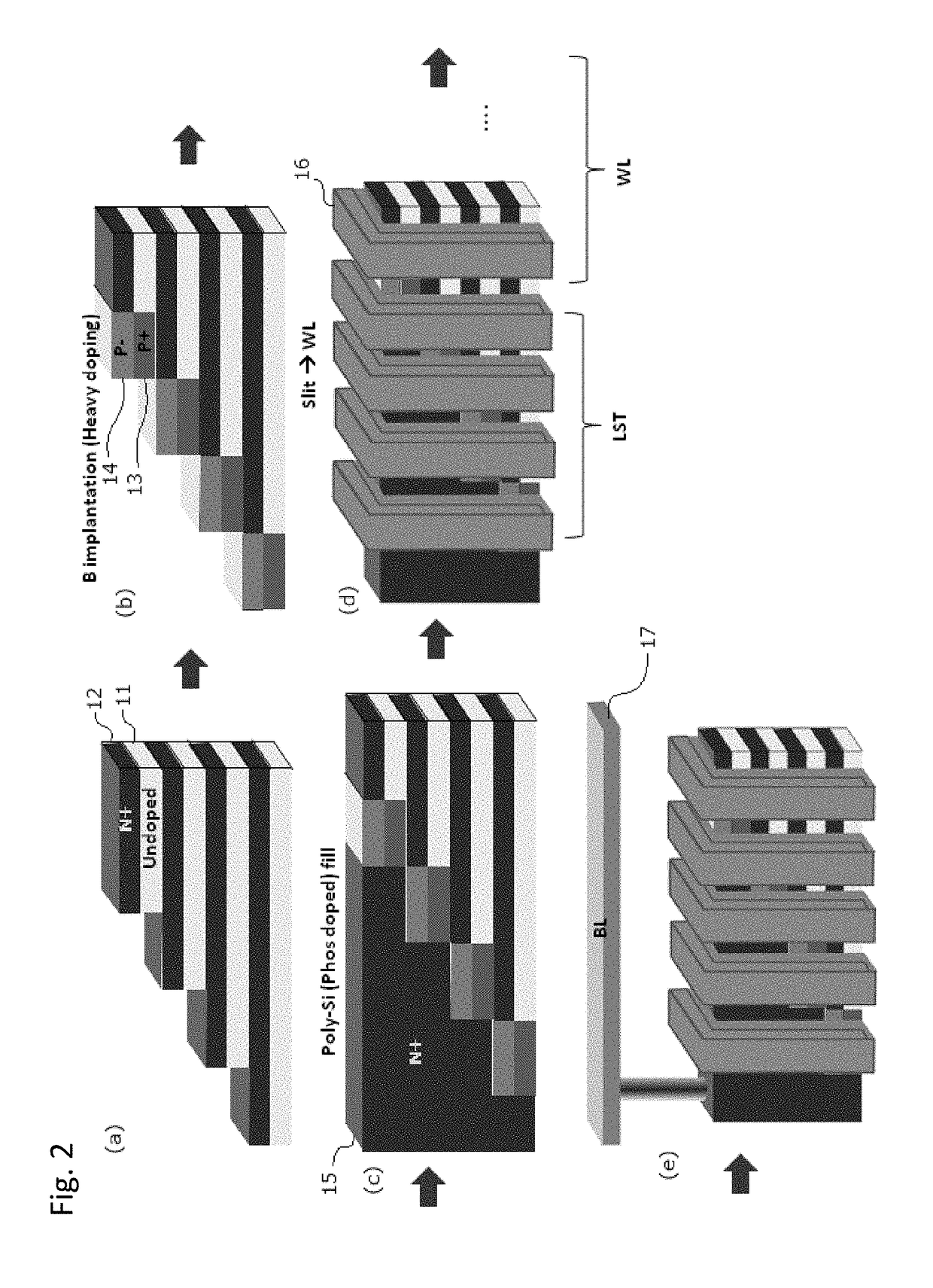
[0062]Undoped Si (or undoped SiGe) layers and phosphorous-doped Si layers were alternately deposited by epitaxial grow processes on a semiconductor substrate wherein the number of stacked layers was about 64. The thickness of the undoped Si (or undoped SiGe) layer was about 50 nm (typically 45 nm to 55 nm) and the thickness of the phosphorous-doped Si layer was about 20 nm (typically 15 nm to 25 nm).

[0063]A staircase was formed in the stacked structure on one side of the stacked structure by patterning, wherein each step of the staircase was constituted by the undoped Si (or undoped SiGe) layer and the phosphorous-doped Si layer. The staircase was formed by: (i) forming a mask (e.g., resist film) in a pattern on the stacked structure of the undoped Si (or undoped SiGe) layers and phosphorous-doped Si layers; (ii) etching the uppermost phosphorous-doped Si layer and undoped Si (or undoped SiGe) layer using the mask to form a step; (iii) etching the mask for next step formation by iso...

example 2

[0068]In Example 2, the staircase was formed on both sides of the stacked structure in the same manner as described in Example 1. Next, boron was doped to each staircase constituted by the phosphorous-doped Si layers and undoped Si (or undoped SiGe) layers by ion implantation at a boron concentration of 1×10¹⁶ / cm2 (typically 5×10¹⁵ / cm2 to 5×10¹⁶ / cm2). Next, the stacked structure was annealed at a temperature of about 1,000° C. (typically 950° C. to 1050° C.) to disperse boron in the phosphorous-doped Si layers and undoped Si (or undoped SiGe) layers.

[0069]Next, a silicon oxide film was deposited on the entire surfaces of the stacked structure with the staircases by CVD, followed by flattening the surface by CMP whereby the space above the staircases was filled with the silicon oxide film as illustrated in (a) in FIG. 3. Next, the silicon oxide film was removed from the space above the staircases by lithography and etching, and then, phosphorous-doped poly-Si was deposited by CVD on ...


PUM


Abstract

In 3D stacked multilayer semiconductor memories including NAND and NOR flash memories, a lightly boron-doped layer is formed on top of a heavily boron-doped layer to form a select transistor, wherein the former serves as a channel of the select transistor and the latter serves as an isolation region which isolates the select transistor from a memory transistor.

Description

BACKGROUNDField of the Invention[0001]The present invention generally relates to 3D stacked multilayer semiconductor memories such as NAND and NOR memories.Description of the Related Art[0002]As 3D stacked multilayer semiconductor memories, several candidates have been pursued, including NAND and NOR memories. One approach is to utilize different types of semiconductors as stacking films. This method is beneficial in that a channel can be formed with a crystal semiconductor that enables much faster operation than a poly-Si channel that is constructed by stacking a poly-Si layer and a SiO layer. One example using such a crystal semiconductor is described in IEDM 2009, p 637-640, by A. Hubert et al. wherein a Si—SiGe stacked structure is utilized. Another example is described in IEEE TRANSACTIONS ON ELECTRON DEVICES, VOL. 58, NO. 4, APRIL 2011, p 1006-1014, by Jan-Gn Yun et al. These two examples focus on NAND flash memories. Other applications including logic circuits are described i...

Claims


Application Information

Patent Timeline
Patent Type & Authority Patents(United States)
IPC IPC(8): H01L27/115H01L27/11578H01L27/11582H01L27/1157
CPCH01L27/11578H01L27/11582H01L27/1157H10B43/50H10B43/20H10B43/27H10B43/35
Inventor OOTSUKA, FUMIO
Owner ASM IP HLDG BV
Why Eureka
Try Eureka