

Silicon carbide semiconductor device
a technology of silicon carbide and semiconductor devices, applied in the field of silicon carbide, can solve problems such as insufficient breakdown voltage structure, and achieve the effect of reducing the number of transistors
- Summary
- Abstract
- Description
- Claims
- Application Information
AI Technical Summary
Benefits of technology
Problems solved by technology
Method used
Image

Examples
first embodiment
[0037]A first embodiment of the present disclosure will be described. In this example, an SiC semiconductor device having MOSFETs of an inversion type trench gate structure will be described as a semiconductor element.
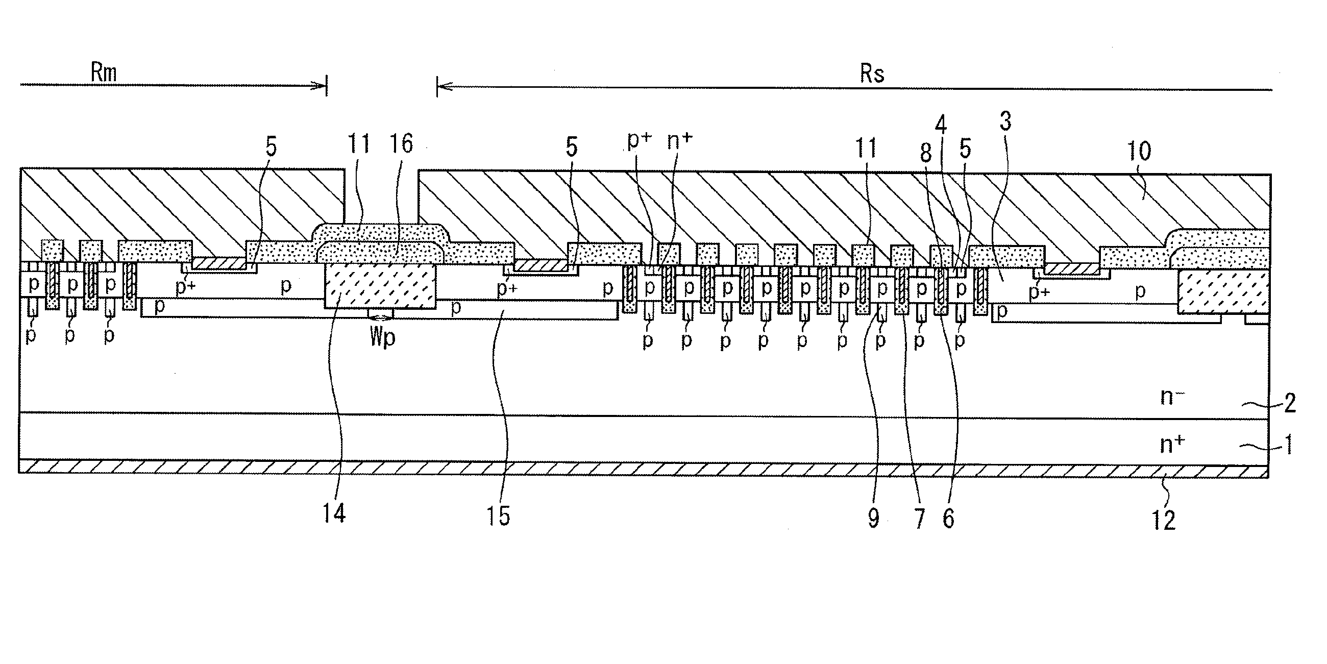
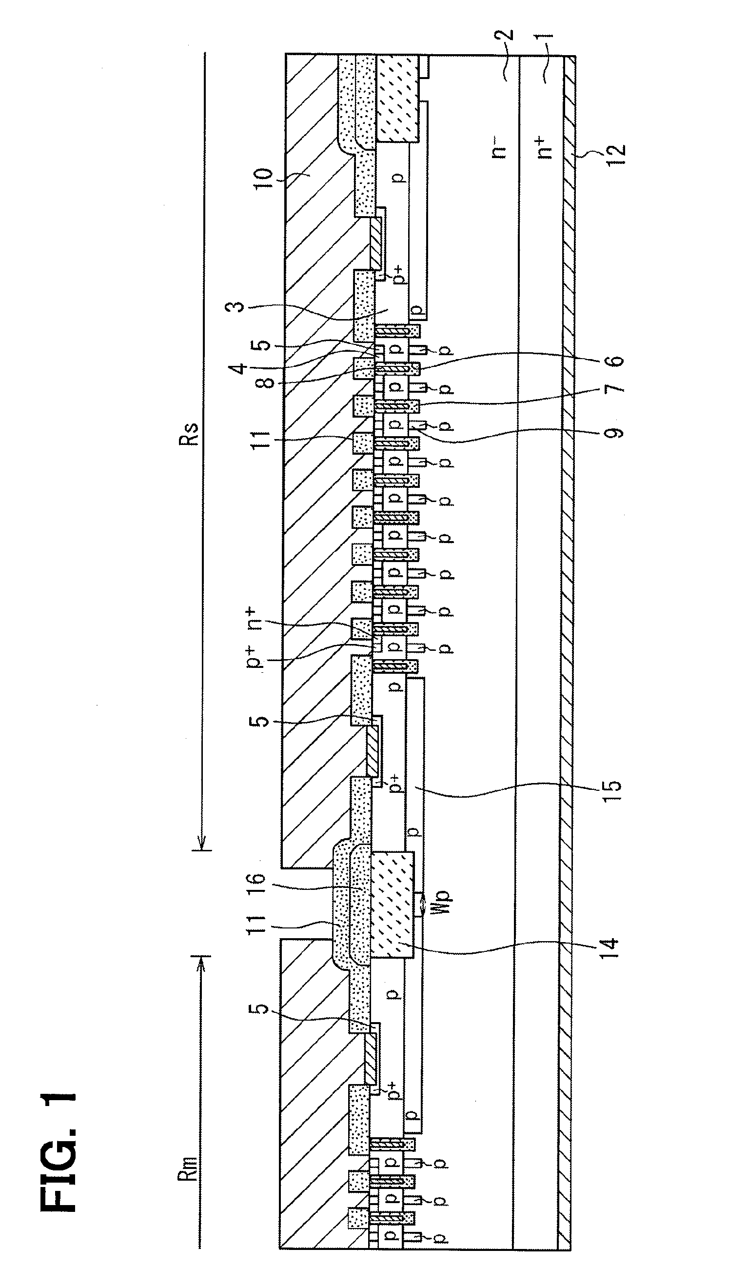
[0038]As illustrated in FIG. 1, the SiC semiconductor device according to this embodiment has a configuration having a region (hereinafter referred to as “main cell region”) Rm forming a main cell and a region (hereinafter referred to as “sense cell region”) Rs forming a sense cell. Those regions Rm and Rs are each provided with an MOSFET of the inversion trench gate structure having the same structure, and the respective regions Rm and Rs are element-isolated from each other, and electrically isolated from each other.
[0039]Specifically, the SiC semiconductor device according to this embodiment is formed of a semiconductor substrate in which an n− type drift layer 2 made of SiC having an impurity concentration lower than that of an n+ type substrate 1 is formed on a su...
second embodiment
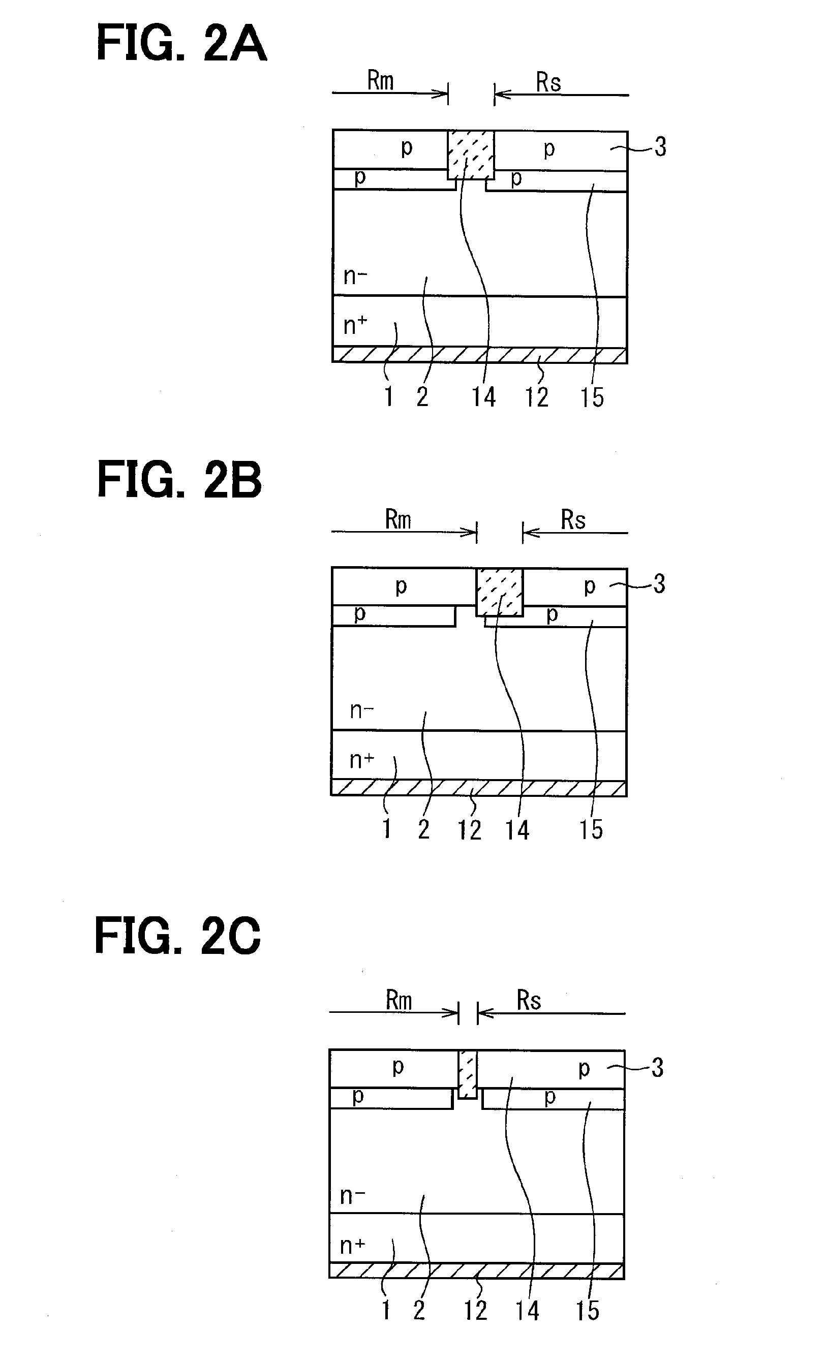
[0067]A second embodiment of the present disclosure will be described. this embodiment is made taking the method of forming the element isolation layer 14 when the off-substrate is used into consideration in the first embodiment. Because a basic structure is identical with that in the first embodiment, only portions different from those in the first embodiment will be described.
[0068]In the SiC semiconductor device, the element formation is performed with the off-substrate to facilitate a step-flow growth. When an off-substrate of which a main surface has an off-angle of a predetermined angle (for example, 4 degrees) is used as the n+ type substrate 1, a state of the surface is inclined by an off-angle and inherited when the n− type drift layer 2 and the p-type base region 3 epitaxially grow on the n+ type substrate 1. That is, the state of the surface is inherited in a direction perpendicular to a just plane of the n+ type substrate 1, but not inherited in a direction perpendicular...
third embodiment
[0074]A third embodiment of the present disclosure will be described. In this embodiment, the process for forming the element isolation layer 14 changes in the first embodiment, and other configurations are identical with those in the first embodiment. Therefore, only portions different from those in the first embodiment will be described.
[0075]A method for manufacturing the SiC semiconductor device according to this embodiment will be described with reference to FIGS. 6A to 6D. Processes other than the process for forming the element isolation layer 14 in the method of manufacturing the SiC semiconductor device according to this embodiment are identical with those in the first embodiment. Therefore, the same portions as those in the first embodiment will be omitted from description with reference to FIGS. 3A to 3C.
[0076]First, in the processes illustrated in FIGS. 6A to 6C, the same processes as those in FIGS. 3A to 3C are performed, the p-type deep layers 9 and the electric field ...
PUM
 Abstract
Description
Claims
Application Information