Capacitive-coupled non-volatile thin-film transistor NOR strings in three-dimensional arrays

a capacitor-coupled, non-volatile technology, applied in transistors, digital storage, instruments, etc., can solve the problems of long latency, limiting the number of transistors that can be programmed in parallel, and unread active tfts that are not read or programmed, so as to reduce read-latency, reduce sensitivities, and increase storage density

Active Publication Date: 2018-11-06
SUNRISE MEMORY CORP
View PDF37 Cites 77 Cited by
  • Summary
  • Abstract
  • Description
  • Claims
  • Application Information

AI Technical Summary

Benefits of technology

[0018]In one embodiment, TFTs are formed using both vertical side edges of each active strip, with vertical local word lines being provided along both the vertical side edges of the active strips. In that embodiment, double-density is achieved by having the local word lines along one of vertical edges of an active strip contacted by horizontal global word lines provided above the active strip, while the local word lines along the other vertical edge of the active strip are contacted by horizontal global word lines provided beneath the active strip. All global word lines may run in a direction transverse to the direction along the lengths of the corresponding active strips. Even greater storage density may be achieved by storing more than one bit of data in each TFT.
[0019]Organizing the TFTs into NOR strings in the memory array—rather than the prior art NAND strings—results in (i) a reduced read-latency that approaches that of a dynamic random access memory (DRAM) array, (ii) reduced sensitivities to read-disturb and program-disturb conditions that are known to be associated with long NAND strings, (iii) reduced power dissipation and a lower cost-per-bit relative to planar NAND or 3-D NAND arrays, and (iv) the ability to read, write or erase TFTs on multiple active strips concurrently to increase data throughput.
[0020]According to one embodiment of the present invention, variations in threshold voltages within NOR strings in a block may be compensated by providing electrically programmable reference NOR strings within the block. Effects on a read operation due to background leakage currents inherent to NOR strings can be substantially eliminated by comparing the sensed result of the TFT being read and that of a concurrently read TFT in a reference NOR string. In other embodiments, the charge-storing element of each TFT may have its structure modified to provide a high write / erase cycle endurance (albeit, a lower data retention time that requires periodic refreshing). In this detailed description, such TFTs having a higher write / erase cycle endurance but a shorter retention time than the conventional memory TFTs (e.g., TFTs in conventional NAND strings) are referred to as being “quasi-volatile.” However, as these quasi-volatile TFTs require refreshing significantly less frequently than a conventional DRAM circuit, the NOR strings of the present invention may be used in lieu of DRAM in some applications. Using the NOR strings of the present invention in DRAM applications allows a substantially lower cost-per-bit figure of merit, as compared to the conventional DRAMs, and a substantially lower read-latency, as compared to conventional NAND strings.

Problems solved by technology

Under this NAND arrangement, the activated TFTs that are not read or programmed may experience undesirable program-disturb or read-disturb conditions.
The low read current that is required to be conducted through a long NAND string results in a long latency.
Channel hot-electron injection programming requires a relatively large electron current to flow through the channel region, therefore limiting the number of transistors that can be programmed in parallel.
Fowler-Nordheim tunneling and direct tunneling are orders of magnitude more efficient than channel hot-electron injection, allowing massively parallel programming; however, such tunneling is more susceptible to program-disturb conditions.

Method used


Image

  • Capacitive-coupled non-volatile thin-film transistor NOR strings in three-dimensional arrays
  • Capacitive-coupled non-volatile thin-film transistor NOR strings in three-dimensional arrays
  • Capacitive-coupled non-volatile thin-film transistor NOR strings in three-dimensional arrays

Examples


Embodiment Construction

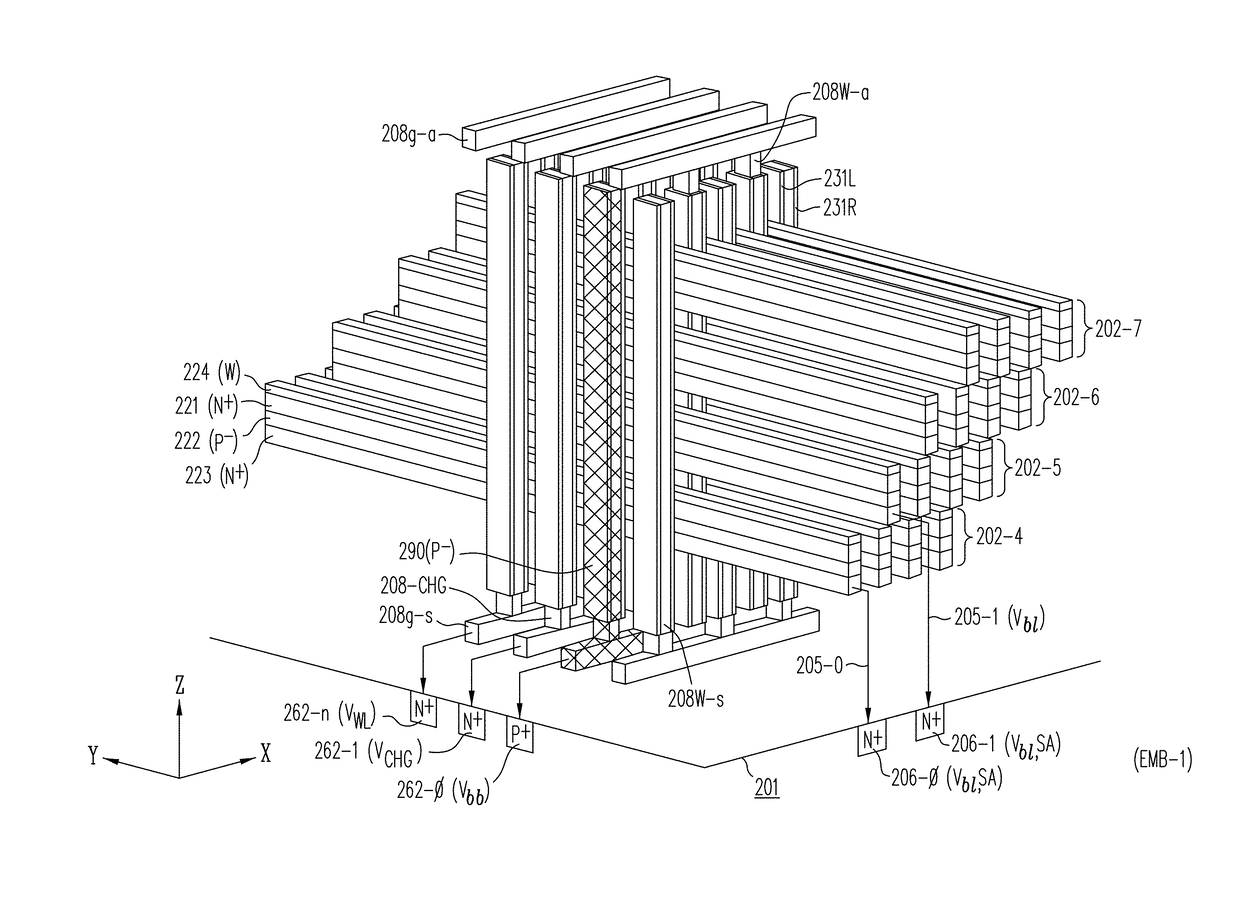
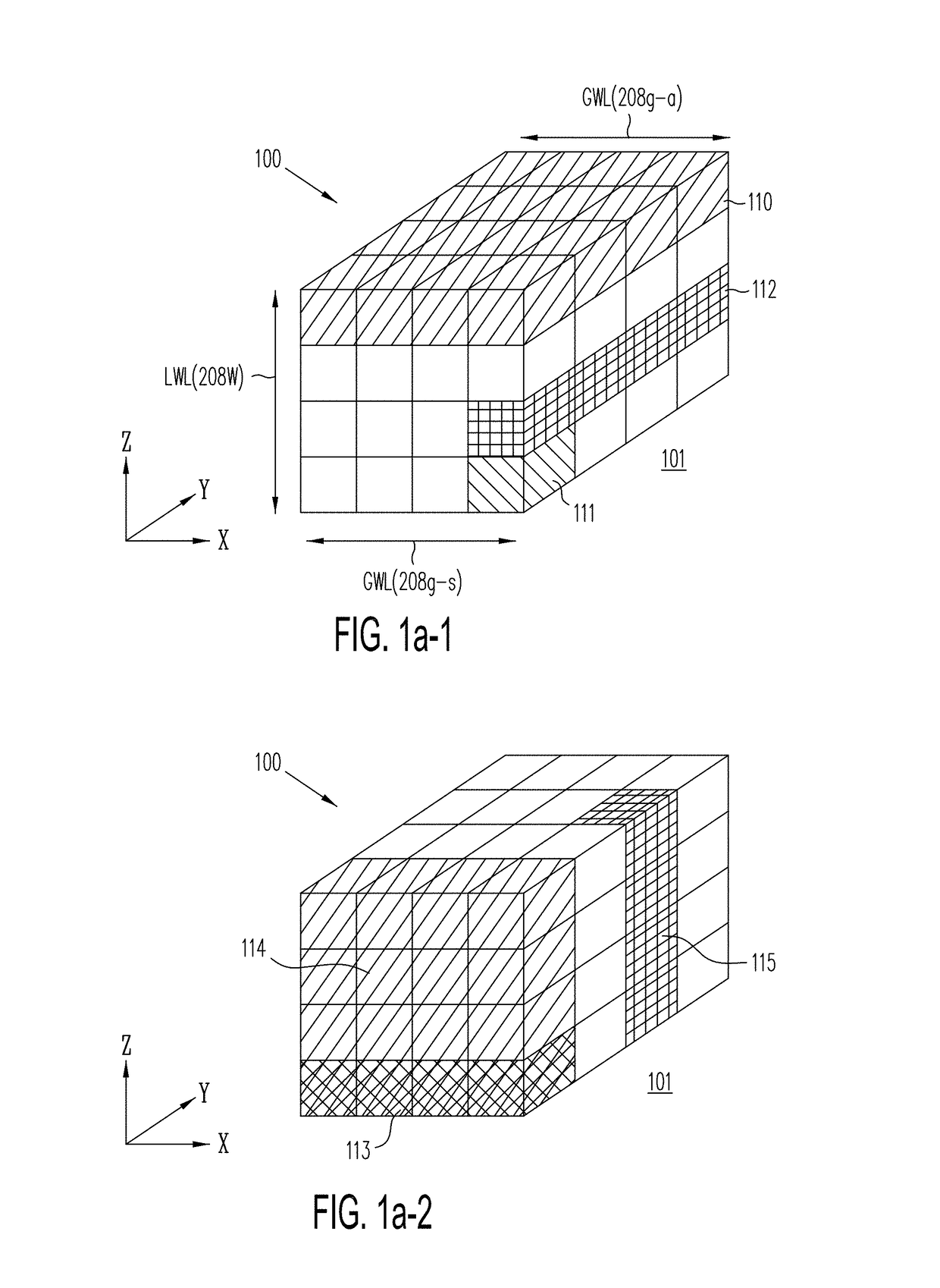
[0067]FIGS. 1a-1 and 1a-2 show conceptualized memory structure 100, illustrating in this detailed description an organization of memory cells according to embodiments of the present invention. As shown in FIG. 1a-1, memory structure 100 represents a 3-dimensional memory array or block of memory cells formed in deposited thin-films fabricated over a surface of substrate layer 101. Substrate layer 101 may be, for example, a conventional silicon wafer used for fabricating integrated circuits, familiar to those of ordinary skill in the art. In this detailed description, a Cartesian coordinate system (such as indicated in FIG. 1a-1) is adopted solely for the purpose of facilitating description. Under this coordinate system, the surface of substrate layer 101 is considered a plane which is parallel to the X-Y plane. Thus, as used in this description, the term “horizontal” refers to any direction parallel to the X-Y plane, while the term “vertical” refers to the Z-direction. As shown, bloc...


PUM


Abstract

Multi-gate NOR flash thin-film transistor (TFT) string arrays are organized as three dimensional stacks of active strips. Each active strip includes a shared source sublayer and a shared drain sublayer that is connected to substrate circuits. Data storage in the active strip is provided by charge-storage elements between the active strip and a multiplicity of control gates provided by adjacent local word-lines. The parasitic capacitance of each active strip is used to eliminate hard-wire ground connection to the shared source making it a semi-floating, or virtual source. Pre-charge voltages temporarily supplied from the substrate through a single port per active strip provide the appropriate voltages on the source and drain required during read, program, program-inhibit and erase operations. TFTs on multiple active strips can be pre-charged separately and then read, programmed or erased together in a massively parallel operation.

Description

CROSS REFERENCE TO RELATED APPLICATIONS[0001]The present invention is related to and claims priority of (i) U.S. provisional application (“Provisional Application I”), Ser. No. 62 / 235,322, entitled “Multi-gate NOR Flash Thin-film Transistor Strings Arranged in Stacked Horizontal Active Strips With Vertical Control Gates,” filed on Sep. 30, 2015; (ii) U.S. provisional patent application (“Provisional Application II”), Ser. No. 62 / 260,137, entitled “Three-dimensional Vertical NOR Flash Thin-film Transistor Strings,” filed on Nov. 25, 2015; (iii) U.S. non-provisional patent application (“Copending Non-Provisional Application”) to which this application is a continuation-in-part of, Ser. No. 15 / 220,375, “Multi-Gate NOR Flash Thin-film Transistor Strings Arranged in Stacked Horizontal Active Strips With Vertical Control Gates,” filed on Jul. 26, 2016; and (vi) U.S. provisional patent application (“Provisional Application III”), Ser. No. 62 / 363,189, entitled “Capacitive Coupled Non-Volati...

Claims


Application Information

Patent Timeline
Patent Type & Authority Patents(United States)
IPC IPC(8): G11C16/34G11C16/04G11C11/56H01L29/10H01L29/08H01L29/92H01L27/11582H01L21/28H01L29/66H01L29/792H01L29/786H01L27/11565
CPCG11C16/3431G11C11/5635G11C11/5642G11C16/0416G11C16/0466G11C16/0483G11C16/0491H01L21/28282H01L27/11582H01L29/0847H01L29/1037H01L29/66833H01L29/78633H01L29/7926H01L29/92G11C11/5628H01L27/11565H01L29/40117H10B43/10H10B43/27G11C16/10
Inventor HARARI, ELI
Owner SUNRISE MEMORY CORP
Why Eureka
Try Eureka