Package structure

a technology of packaging structure and chip, applied in the direction of semiconductor devices, semiconductor/solid-state device details, electrical equipment, etc., can solve the problems of complex process steps, less readily achieved fine pitch demand, and higher process cost of sputtering, so as to achieve simplified process and reduce production cost

Inactive Publication Date: 2018-11-20
IBIS INNOTECH
View PDF2 Cites 1 Cited by
  • Summary
  • Abstract
  • Description
  • Claims
  • Application Information

AI Technical Summary

Benefits of technology

[0005]An embodiment of the disclosure provides a package structure that can directly form a circuit on an insulator such that process can be simplified and production cost can be reduced to better meet the demands of fine pitch.
[0036]Based on the above, in a package structure of an embodiment of the disclosure, comprehensive chemical plating may first be performed on the insulator to form a metal layer covering the outer surface of the insulator, and then a first groove is formed on the metal layer by a means such as laser, plasma, or a mechanical tool to electrically insulate the circuit portion from the rest of the metal layer to form the patterned metal layer. Therefore, the surface of the insulator exposed after carving is lower than the outer surface of the insulator covered by the patterned metal layer. Moreover, the manufacturing process of the package structure can be effectively simplified. Also, the package structure formed by the manufacturing process can solve the issue of failing to reduce circuit pitch due to plated copper overflow at the circuit edge during the process of forming circuit by laser carving.
[0037]Moreover, the rest of the patterned metal layer outside the circuit portion covers a large area of the surface of the insulator, and can therefore be used for grounding / shielding to reduce the effects of electrostatic discharge and electromagnetic interference. Moreover, the insulator of an embodiment of the disclosure can be formed by molding, and therefore the insulator has greater design flexibility in terms of thickness and appearance. Therefore, not only can the design flexibility of the package structure of the disclosure be increased, the criteria of fine pitch can be more readily met. Also, the manufacturing process can be effectively simplified and the production cost and overall thickness of the package structure can be reduced.

Problems solved by technology

However, the steps of the process are complex, and the process cost of sputtering is higher.
Moreover, a patterned circuit layer forming by using a patterned dry layer as an electroplating barrier less readily achieves the current demand for fine pitch.
Moreover, the material of the insulator mostly adopts polyimide or Ajinomoto build-up film (ABF) resin, and the cost thereof is higher.
Therefore, the manufacture of the current package substrate is not only complex, but also costly.

Method used


Image

  • Package structure
  • Package structure
  • Package structure

Examples


Embodiment Construction

[0055]The foregoing and other technical contents, features, and effects of the embodiments of the disclosure are intended to be described more comprehensively in each of the following embodiments accompanied with figures. In the following embodiments, terms used to indicate direction such as “up,”“down,”“front,”“back,”“left,” and “right”, merely refer to directions in the accompanying figures. Therefore, the directional terms are used to illustrate and are not intended to limit the embodiments of the disclosure. Moreover, in each of the embodiments below, the same or similar reference numerals are used for the same or similar devices.

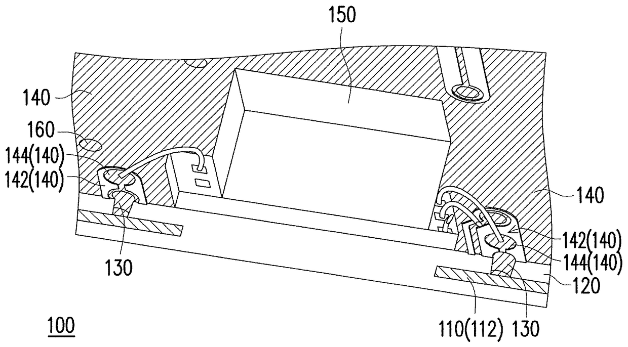
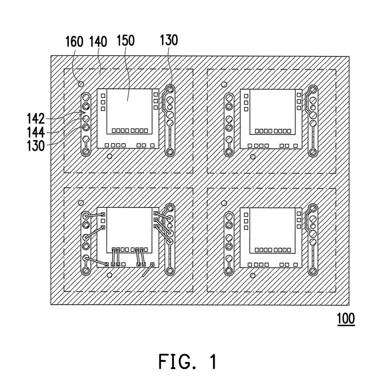
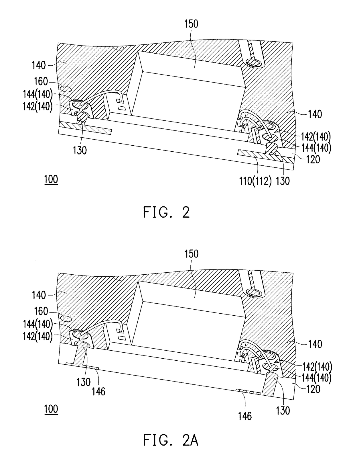
[0056]FIG. 1 is a top schematic of a package structure according to an embodiment of the disclosure. FIG. 2 is a cross-sectional schematic of a portion of a package structure according to an embodiment of the disclosure. Referring to both FIG. 1 and FIG. 2, in the present embodiment, a package structure 100 includes a lead frame 110, an insulator 120, a...


PUM


Abstract

A package structure includes a lead frame, an insulator, a plurality of conductive vias, a patterned metal layer, and a chip. The lead frame includes a plurality of contacts. The insulator covers the lead frame. The conductive vias are disposed on the insulator and connected to the contacts. The patterned metal layer covers an outer surface of the insulator and includes a groove and a circuit portion. The circuit portion is connected to and covers the conductive vias and contacts. The groove surrounds the circuit portion such that the circuit portion is electrically insulated from the rest of the patterned metal layer. A surface of the insulator exposed by the groove is lower than the outer surface. The chip is disposed on the insulator and electrically connected to the circuit portion.

Description

CROSS-REFERENCE TO RELATED APPLICATION[0001]This application claims the priority benefit of Taiwan application serial no. 106111723, filed on Apr. 7, 2017. The entirety of the above-mentioned patent application is hereby incorporated by reference herein and made a part of this specification.BACKGROUNDTechnical Field[0002]The embodiments of the disclosure relate to a package structure, and more particularly, to a package structure of a chip.Description of Related Art[0003]In today's information society, human dependence on electronic products is increasing. To meet the demands for high speed, high performance, and lightweight and compact design of current electronic products, a flexible circuit board having flexible properties is gradually applied in various electronic apparatuses such as: mobile phones, notebook PCs, digital cameras, tablet PCs, printers, and disk players.[0004]In general, the manufacture of a circuit board mainly includes performing a pre-treatment, sputtering, cop...

Claims


Application Information

Patent Timeline
Patent Type & Authority Patents(United States)
IPC IPC(8): H01L23/495H01L23/498H01L23/00
CPCH01L23/49861H01L23/49811H01L23/49827H01L23/49838H01L23/49894H01L24/16H01L24/48H01L2224/48235H01L23/4952H01L23/49531H01L23/49833H01L2224/16227H01L2224/16235H01L2224/48227H01L23/49822H01L23/495H01L24/49H01L2224/16145H01L2224/16146H01L2224/16245H01L2224/48245H01L2224/49173H01L2224/85411H01L2224/85439H01L2224/85444H01L2224/85447H01L2224/85464H01L2224/85466H01L2224/85484H01L2224/85472H01L23/49548H01L2924/181H01L2924/15153H01L23/13H01L2924/00014
Inventor LIU, WEN-CHUNLAI, WEI-JEN
Owner IBIS INNOTECH
Why Eureka
Try Eureka