Semiconductor package and fabrication method thereof

a technology of semiconductor packages and fabrication methods, applied in the direction of semiconductor devices, semiconductor/solid-state device details, electrical apparatus, etc., can solve the problems of thermal stress formed between the semiconductor package and the printed circuit board, further reduction of the package size, and degrading the quality of electrical connections, so as to reduce thermal stress, increase the amount of solder, and improve the reliability of the electronic product

Active Publication Date: 2009-12-29
SILICONWARE PRECISION IND CO LTD
View PDF4 Cites 30 Cited by
  • Summary
  • Abstract
  • Description
  • Claims
  • Application Information

AI Technical Summary

Benefits of technology

[0014]It is another objective of the present invention to provide a non-carrier type semiconductor package and a fabrication method thereof, which is capable of reducing the thermal stress of a plurality of solder joints that connect the semiconductor package with a printed circuit board, thereby enhancing the reliability of the electronic products.
[0015]It is a further objective of the present invention to provide a non-carrier type semiconductor package and a fabrication method thereof, which is capable of avoiding the problem of short circuit caused by the neighboring solder contact due to the improper control over mounting between the semiconductor package and the printed circuit board, thereby preventing defects during fabrication.
[0016]It is still another objective of the present invention to provide a semiconductor package and a fabrication method thereof, which is capable of effectively enhancing the semiconductor package circuit layout flexibility and the electrical connection quality.
[0019]Therefore, the semiconductor package of the present invention can be electrically connected to an external device, such as a printed circuit board, through bump structure between the conductive metallic layers of the semiconductor package and the printed circuit board with an increased distance between the semiconductor package and the printed circuit board, as well as reduced thermal stress caused by a difference between the thermal expansion coefficients of the semiconductor package and the printed circuit board. As a result, the reliability of the electronic product can be enhanced without increasing the solder amount for electrical connection, and the problem of short circuit caused by a contact between neighboring bonding wire due to increased solder amount can be avoided.
[0020]Furthermore, the semiconductor package of the present invention does not need a chip carrier (such as a prepared lead frame or substrate), so as to lower the production cost and meet the demands for light-weighted and low profiled electronic products. The patterned circuit layer formed in the semiconductor package can be flexibly laid out in corresponding to the degree of chip integration and be positioned closer to the region where an electrical connection with the chip occurs, so as to shorten the loop length of the bonding wire that electrically connects the chip to the patterned circuit layer, and to shorten the electrical connection path, thereby enhancing the circuit layout flexibility and electrical connection quality of the semiconductor package.

Problems solved by technology

In addition, with the increasing demands for light-weighted and low-profiled semiconductor packages, the conventional lead frame based semiconductor package can not meet the demand for a further reduction in package size, therefore the industry has developed a non-carrier type semiconductor package that the overall thickness of the package can be reduced significantly by eliminating the use of a lead frame.
However, when a highly integrated chip, namely, the chip has a high density layout of electronic elements is used in the aforementioned QFN semiconductor package and the non-carrier type semiconductor package, comparatively large numbers of leads or electroplating solder pads for the corresponding electrical connections are required, and as a result, the package size need to increase to accommodate more I / O and then the loop length of the bonding wires and the distance between the chip and the leads or the electroplating solder pads are increased, and consequently, not only increase the difficulties of bonding wire operation, but also easily cause problems such as bonding wire shift and short circuit, thus seriously degrading the quality of electrical connections.
However, regardless of the aforementioned QFN or non-carrier type semiconductor packages, when the semiconductor package is electrically connected to the printed circuit board by means of the surface mounting technology (SMT) via the reflowed solder forming the solder joints, due to the different materials of the semiconductor package and the printed circuit board, there is a thermal stress formed between the semiconductor package and the printed circuit board.
Consequently, in the aforementioned semiconductor package of the prior art, since the solder joint height is very low, the solder joint would suffer a great amount of thermal stress.
In this situation, it would not only reduce the fatigue life of the solder joint, but further cause the problem of crack of the solder joint, therefore seriously affecting the reliability of the electronic products.
Comparatively, when the height and amount of the solder are increased, the excessive amount of solder or improper control over mounting between the semiconductor package and the printed circuit board would cause neighboring solder to contact each other which would further cause short circuit and bring defects in fabrication.

Method used


Image

  • Semiconductor package and fabrication method thereof
  • Semiconductor package and fabrication method thereof
  • Semiconductor package and fabrication method thereof

Examples


first preferred embodiment

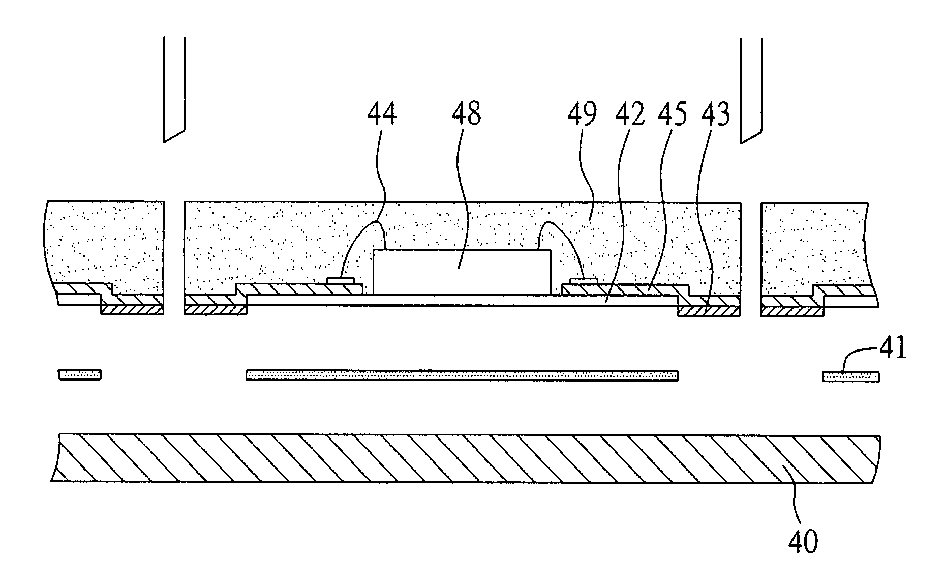
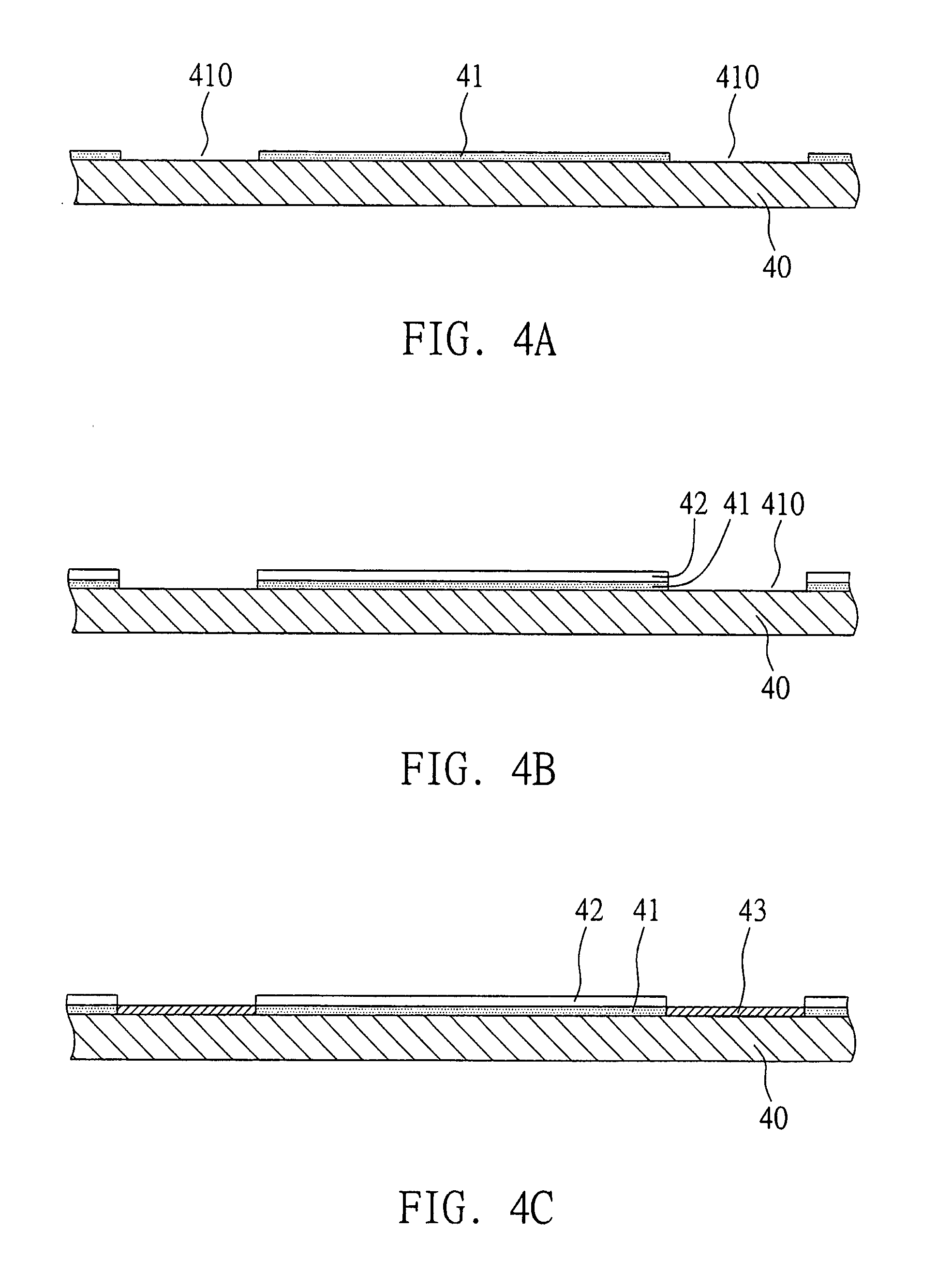
[0029]FIGS. 4A-4G are cross-sectional views showing a semiconductor package and a fabrication method thereof according to the first preferred embodiment of the present invention.

[0030]As shown in FIG. 4A, a metal carrier 40, e.g. a copper (Cu) plate is prepared, and then a sacrificial layer 41 is applied on a surface of the metal carrier. The sacrificial layer 41 is made of, for example, polymeric material, such as epoxy resin, photo-resist, etc., and its thickness is about 10 to 30 μm. The sacrificial layer 41 has a plurality of through holes 410, formed by means of traditional photolithography, or stencil printing method.

[0031]As shown in the FIG. 4B, an insulation layer 42 is applied on the sacrificial layer 41. The insulation layer 42 is, for example, a solder mask, and is treated by photolithography to expose the through holes 410 of the sacrificial layer 41 and to further expose the metal carrier 40. Alternatively, a laser perforation process is performed on the sacrificial la...

second embodiment

The Second Embodiment

[0039]FIG. 5A and FIG. 5B are cross-sectional views illustrating a semiconductor package according to a second preferred embodiment of the present invention. As shown in FIG. 5A, the semiconductor package of the present embodiment is substantially similar to the one in the first embodiment, with only the major difference being that the chip 58 of the present embodiment is mounted on the patterned circuit layer 55 by means of flip-chip. More specifically, in the chip mounting process, the active surface of the chip 58 is facing towards the patterned circuit layer 55 to be electrically connected to the plurality of terminals 550 of the patterned circuit layer 55 or the metallic layers 56 formed on the terminals 550 via a plurality of solder bumps 54. Then, an encapsulant 59 for encapsulating the chip 58 is formed. Compared with the bonding wires that connect the chip and the patterned circuit layer, the flip-chip technology using solder bumps further shortens the ...


PUM

PropertyMeasurementUnit
thicknessaaaaaaaaaa
thicknessaaaaaaaaaa
conductiveaaaaaaaaaa

Abstract

A semiconductor package and a fabrication method are disclosed. The fabrication method includes applying a sacrificial layer on one surface of a metal carrier, applying an insulation layer on the sacrificial layer, and forming through holes in the sacrificial layer and the insulation layer to expose the metal carrier; forming a conductive metallic layer in each through hole; forming a patterned circuit layer on the insulation layer to be electrically connected to the conductive metallic layer; mounting at least a chip on the insulation layer and electrically connecting the chip to the patterned circuit layer; forming an encapsulant to encapsulate the chip and the patterned circuit layer; and removing the metal carrier and the sacrificial layer to expose the insulation layer and conductive metallic layer to allow the conductive metallic layer to protrude from the insulation layer. In the present invention, the distance between the semiconductor package and the external device is increased, and thermal stress caused by difference between the thermal expansion coefficients is reduced, so as to enhance the reliability of the product.

Description

BACKGROUND OF THE INVENTION[0001]1. Field of the Invention[0002]The present invention generally relates to semiconductor packages and fabrication methods thereof, and more particularly to a non-carrier type semiconductor package and a fabrication method thereof.[0003]2. Description of the Prior Art[0004]Conventionally, a semiconductor package is often formed by using a lead frame as a chip carrier. The leadframe comprises a die pad and a plurality of leads formed around the periphery of the die pad. The lead-frame based semiconductor package is formed by attaching a semiconductor chip to the die pad and electrically connecting the semiconductor chip to the leads via the bonding wires, followed by forming an encapsulant to encapsulate the chip, die pad, bonding wires and the inner portions of the leads.[0005]There are a great variety of lead frame based semiconductor packages, such as quad flat non-leaded (QFN) semiconductor package. The main characteristic feature of this QFN semico...

Claims


Application Information

Patent Timeline
Patent Type & Authority Patents(United States)
IPC IPC(8): H01L23/48H01L23/52H01L29/40
CPCH01L21/561H01L23/3121H01L24/97H01L21/6835H01L2224/48247H01L2221/68345H01L2224/16H01L2224/48091H01L2224/97H01L2924/01013H01L2924/01029H01L2924/01046H01L2924/01047H01L2924/01078H01L2924/01079H01L2924/01082H01L2924/18161H01L2924/01033H01L24/48H01L2224/85H01L2224/81H01L2924/00014H01L2924/351H01L2924/15747H01L2924/181H01L2924/00011H01L2924/00H01L2224/0401H01L2924/00012H01L2224/45099H01L2224/45015H01L2924/207
Inventor JIANG, YIH-JENNPU, HAN-PINGHUANG, CHIEN-PINGHSIAO, CHENG-HSU
Owner SILICONWARE PRECISION IND CO LTD
Why Eureka
Try Eureka