Method for forming patterns of semiconductor device

a semiconductor device and pattern technology, applied in the direction of semiconductor devices, electrical devices, transistors, etc., can solve the problems that conventional photolithography technologies encounter difficulties in the fabrication of nano-sized fine patterns, and achieve the effect of smaller uniform diameter and larger compactness in layout unit area

Active Publication Date: 2018-12-18
UNITED MICROELECTRONICS CORP +1
View PDF50 Cites 0 Cited by
  • Summary
  • Abstract
  • Description
  • Claims
  • Application Information

AI Technical Summary

Benefits of technology

[0006]An unconventional photolithography method is accordingly provided in the present invention based on using the self-assembled material to form semiconductor patterns. The advantage and creativity of present invention is to manufacture semiconductor devices, such as a memory cell, with larger compactness in layout unit area and uniform diameter smaller than current photolithographic resolution limit without using expensive advanced photolithographic equipment or additional complicated processes.

Problems solved by technology

However, conventional photolithography technologies encounter difficulties in the fabrication of nano-sized fine patterns, in particular, nano-sized fine patterns of less than about 20 nm, due to the wavelength resolution limit.

Method used


Image

  • Method for forming patterns of semiconductor device
  • Method for forming patterns of semiconductor device
  • Method for forming patterns of semiconductor device

Examples


Embodiment Construction

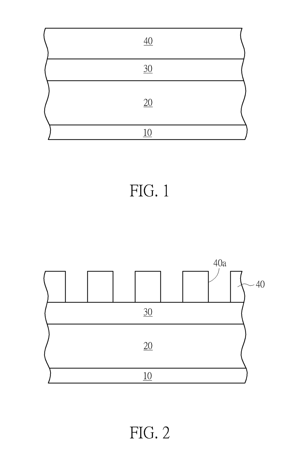
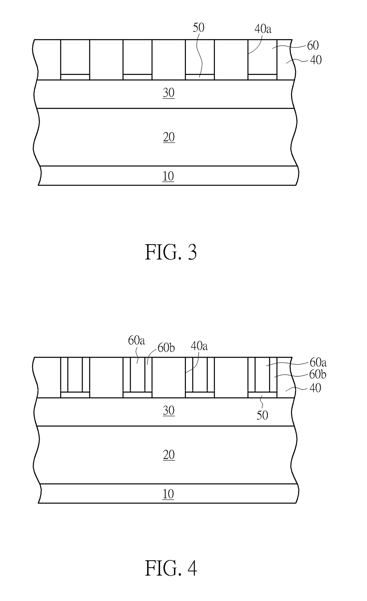
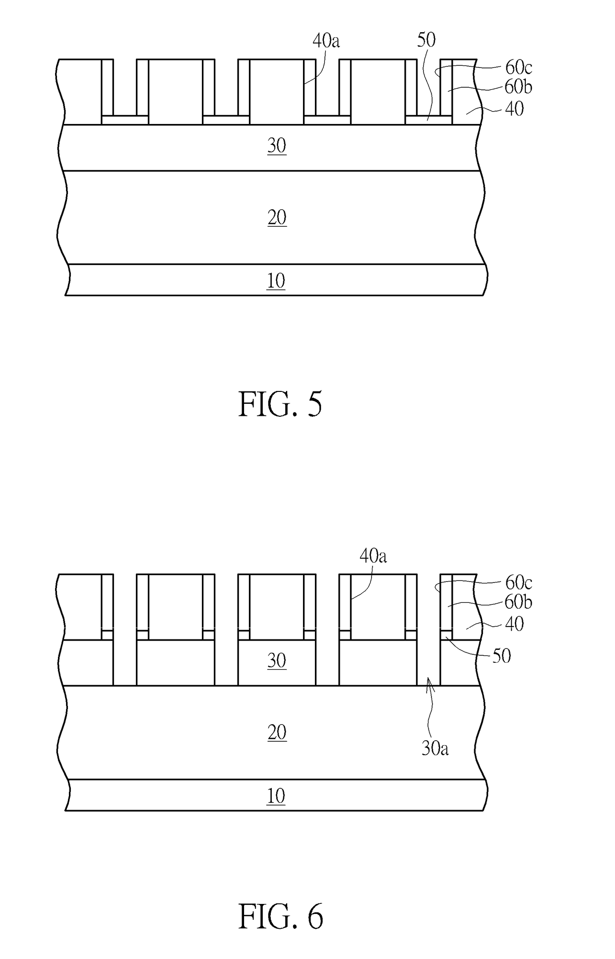
[0014]In the following detailed description of the present invention, reference is made to the accompanying drawings which form a part hereof and is shown by way of illustration and specific embodiments in which the invention may be practiced. These embodiments are described in sufficient details to enable those skilled in the art to practice the invention. Other embodiments may be utilized and structural, logical, and electrical changes may be made without departing from the scope of the present invention. The following detailed description, therefore, is not to be taken in a limiting sense, and the scope of the present invention is defined by the appended claims.

[0015]It will be understood that, although the terms first, second, etc. may be used herein to describe various elements, components, regions, layers and / or sections, these elements, components, regions, layers and / or sections should not be limited by these terms. These terms are only used to distinguish one element, compo...


PUM


Abstract

A method for forming patterns of semiconductor device is provided in the present invention, with steps of filling up first self-assembly material in first openings in a dielectric layer, phase-separating the first self-assembly material to form a first portion and a second portion surrounding the first portion, removing the first portion and performing a first etch process to form a first mask pattern in a mask layer, forming a second dielectric layer and repeating the above steps to form a second mask pattern in the mask layer, wherein the second mask pattern is aligned with the first mask pattern to form a common mask pattern.

Description

BACKGROUND OF THE INVENTION[0001]1. Field of the Invention[0002]The invention relates generally to a method for forming patterns of semiconductor device, and more particularly, to a method of using a self-assembling process to form patterns of semiconductor device.[0003]2. Description of the Prior Art[0004]Recently, in view of the decrease in size of electronic devices and the increase in the degree of integration of semiconductor devices, there has been an increased demand for lithography technologies of forming fine nano-sized patterns. However, conventional photolithography technologies encounter difficulties in the fabrication of nano-sized fine patterns, in particular, nano-sized fine patterns of less than about 20 nm, due to the wavelength resolution limit. Accordingly, various methods based on new principles for fabricating nano-sized fine patterns have been studied in the semiconductor industry. One of these methods utilizes a self-assembled nano-structure.[0005]The self-ass...

Claims


Application Information

Patent Timeline
Patent Type & Authority Patents(United States)
IPC IPC(8): H01L21/311H01L21/027H01L21/02H01L21/033H01L27/108
CPCH01L21/0338H01L21/0273H01L21/02118H01L21/02356H01L21/0337H01L21/31144H01L21/0332H01L27/10823H01L27/10814H10B12/033H10B12/34H10B12/315
Inventor CHEN, KAI-PINGYU, KUEI-HSUANYEH, CHIU-HSIENFENG, LI-WEI
Owner UNITED MICROELECTRONICS CORP
Why Eureka
Try Eureka