Method for fabricating a charging device

Active Publication Date: 2019-02-19
EASTMAN KODAK CO
View PDF36 Cites 0 Cited by
  • Summary
  • Abstract
  • Description
  • Claims
  • Application Information

AI Technical Summary

Benefits of technology

The invention offers a charging device with high accuracy in positioning the charging electrode, achieved by using a conductive trace and a base layer deposited without needing photomasking. Additionally, the device has an internal heater that is encapsulated and in excellent thermal contact with the ceramic charging device, allowing for lower power usage and reduced distortion.

Problems solved by technology

Deviations in charging electrode flatness across the length of the nozzle array can therefore result in variation in impact height of the non-print drops on the catcher.
Such variations in impact height tend to reduce the operating latitude of the printhead.
As noted in commonly-assigned U.S. Pat. No. 7,163,281, the heating of the charging device to prevent condensation on the charging device can thermally deform the charging device altering the spacing between the charging electrode and the liquid streams, and thereby affecting the operating latitude of the printhead.
Failure to remove ink from this space can result in electrical shorting conditions between any exposed conductive traces on the upper surface of the charging device and other conductive surface in the printhead.
These types of shorting conditions often result in printhead errors and premature printhead failure.
While such insulating layers do provide protection for the conductive traces on the charging device, the presence of the insulating layer on the upper surface of the charging device reduces the size of the gap between the charging device and the nozzle plate which can further impede the removal of ink from the gap between the charging device and the nozzle plate.
Furthermore, under prolonged exposure to the ink, the insulating epoxy layers have been found to degrade.

Method used


Image

  • Method for fabricating a charging device
  • Method for fabricating a charging device
  • Method for fabricating a charging device

Examples


Embodiment Construction

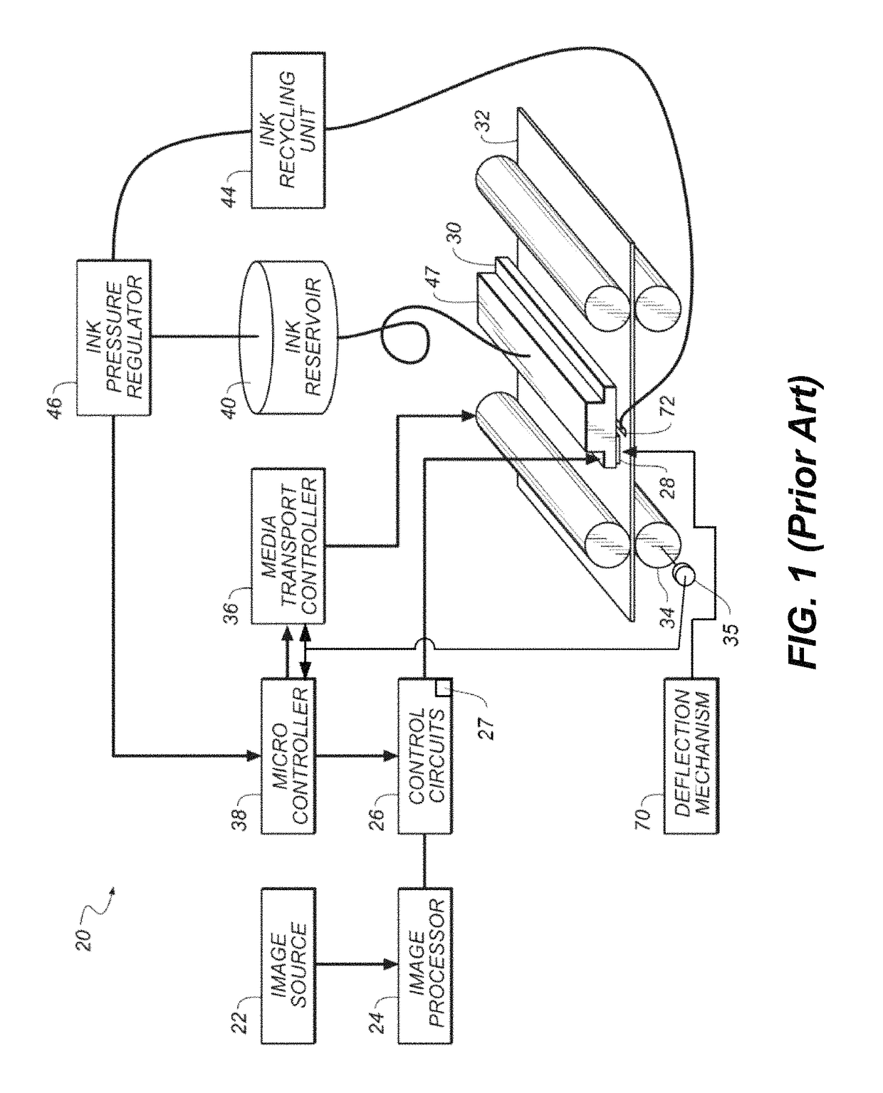
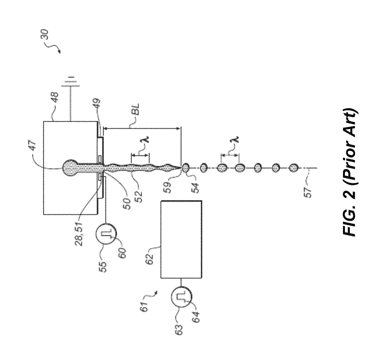
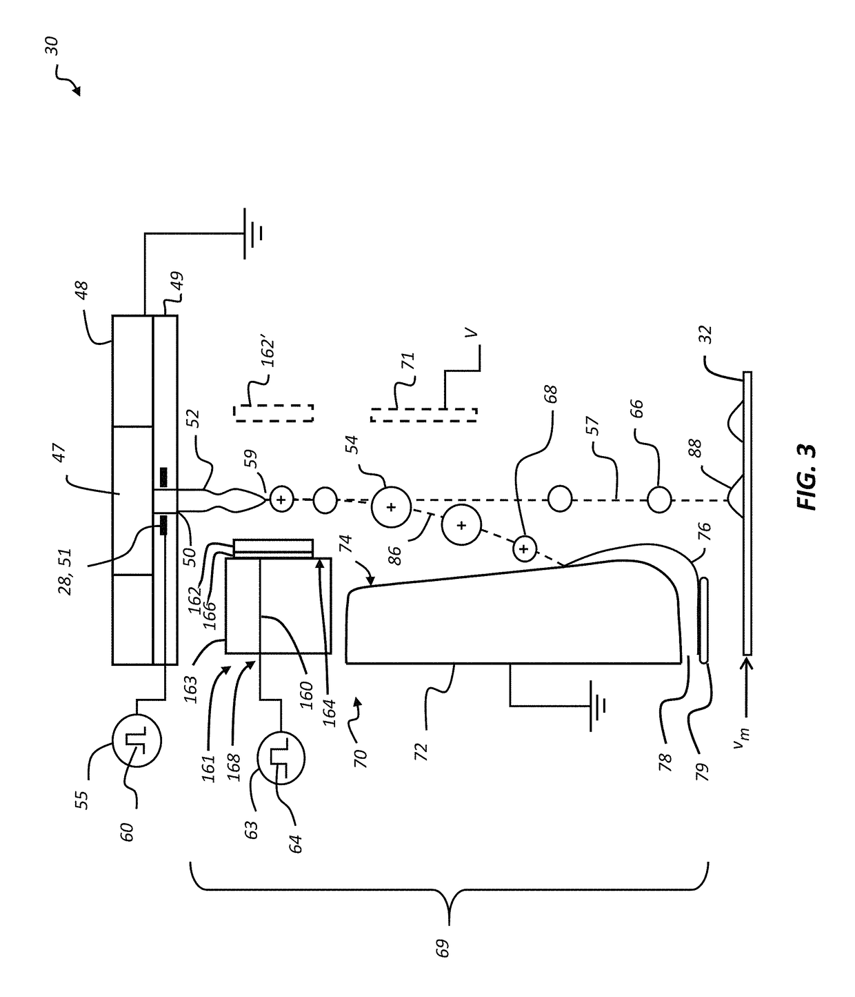
[0027]The present description will be directed in particular to elements forming part of, or cooperating more directly with, apparatus in accordance with the present invention. It is to be understood that elements not specifically shown or described may take various forms well known to those skilled in the art. References to “a particular embodiment” and the like refer to features that are present in at least one embodiment of the invention. Separate references to “an embodiment” or “particular embodiments” or the like do not necessarily refer to the same embodiment or embodiments; however, such embodiments are not mutually exclusive, unless so indicated or as are readily apparent to one of skill in the art. The use of singular or plural in referring to the “method” or “methods” and the like is not limiting. It should be noted that, unless otherwise explicitly noted or required by context, the word “or” is used in this disclosure in a non-exclusive sense.

[0028]The example embodiment...


PUM


Abstract

A method of fabricating a charging device for an inkjet printing system includes providing a charging device body having at least one conductive trace passing through the interior of the charging device body connecting between a charging face of the charging device body and an interconnection region remote from the charging face. A portion of the at least one conductive trace is exposed on the charging face. A vapor deposition process is used to deposit a conductive base layer through a shadow mask onto the charging face, wherein the deposited conductive base layer contacts the exposed portion of at least one conductive trace. One or more conductive metallic layers are plated onto the deposited conductive base layer to form a charging electrode.

Description

FIELD OF THE INVENTION[0001]This invention relates generally to the field of digitally-controlled printing devices, and in particular to charging electrodes for use in continuous printing systems in which a liquid stream breaks into printing drops and non-printing drops, wherein the non-printing drops are charged and deflected away from a printing drop trajectory.BACKGROUND OF THE INVENTION[0002]Continuous inkjet printing is a printing technology that is well suited for high-speed printing applications, having high throughput and low cost per page. Recent advances in continuous inkjet printing technology have included thermally induced drop formation, which is capable of selectively altering the drop breakoff phase relative to a periodic charging electrode waveform and thereby controlling whether the drop is charged or uncharged, and electrostatic deflection of charged drops to separate the charged non-print drops from the uncharged print drops. These advances have enabled the print...

Claims


Application Information

Patent Timeline
IPC IPC(8): B41J2/02B41J2/16
CPCB41J2/162B41J2/1642B41J2/03B41J2/175B41J2202/22B41J2/08B41J2/085B41J2/09
Inventor SIMON, ROBERT J.BAUMER, MICHAEL FRANKHARRISON, JR., JAMES E.MORRIS, BRIAN GEORGERIKE, CHARLES D.
Owner EASTMAN KODAK CO
Why Eureka
Try Eureka