Interconnect element circuitry for RF electronics

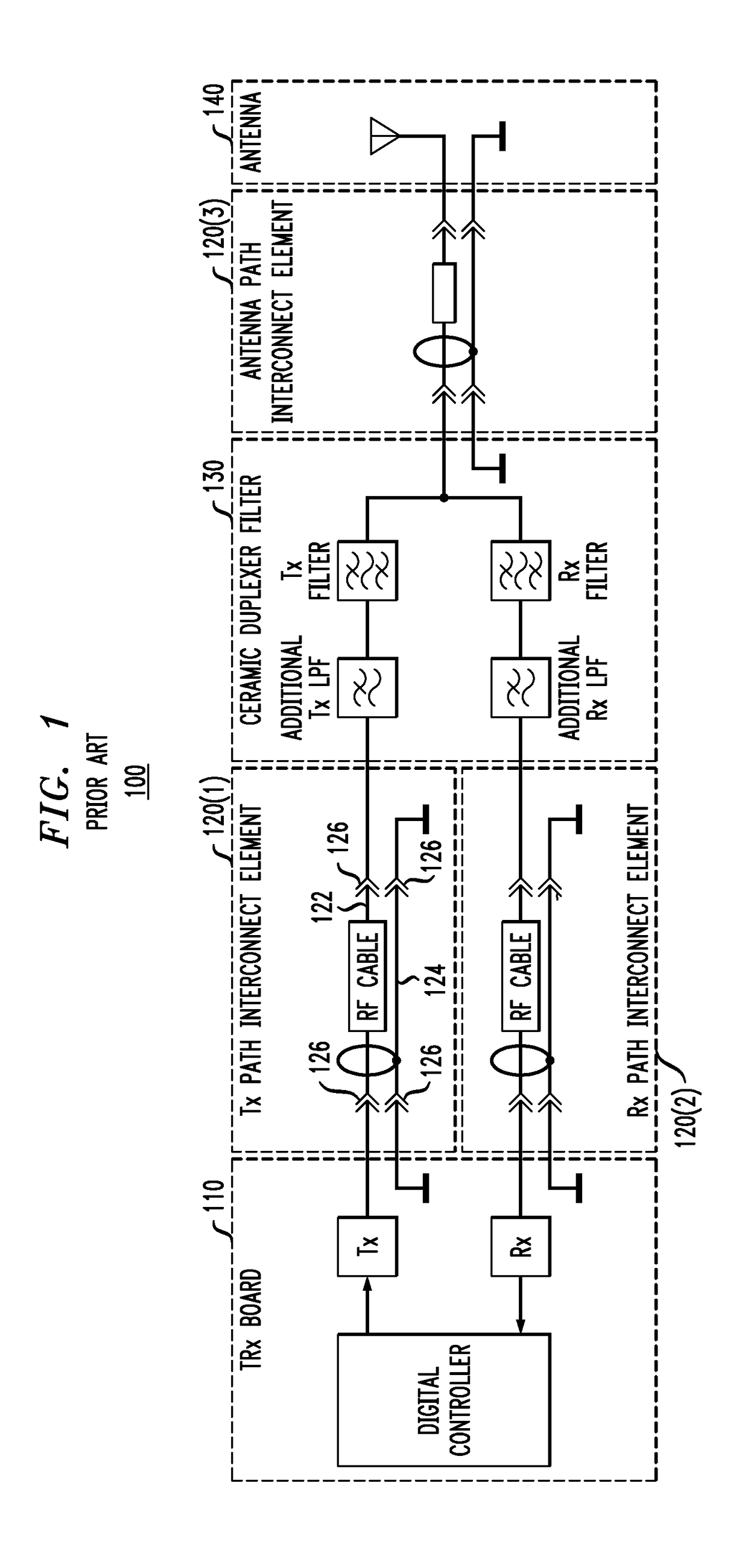
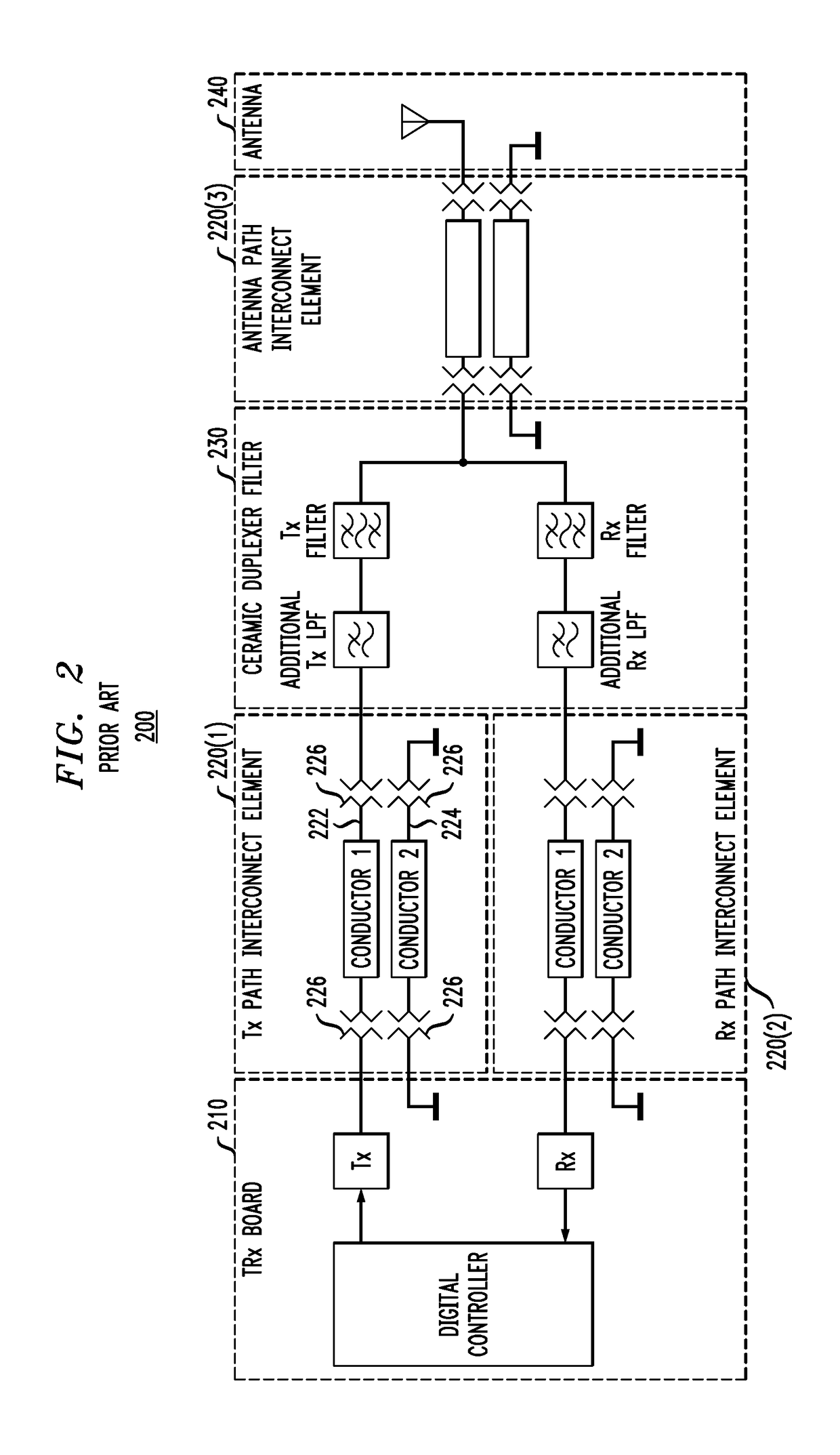
a technology of interconnect elements and electronics, applied in the field of rf (radio frequency) electronics, can solve the problems of wideband rf connectors, interconnect elements b>120/b>, and high-power rf filters that are not typically produced, and achieve high stop-band attenuation, low pass-band insertion loss, and good impedance matching

Active Publication Date: 2019-02-26
NOKIA SOLUTIONS & NETWORKS OY
View PDF5 Cites 0 Cited by
  • Summary
  • Abstract
  • Description
  • Claims
  • Application Information

AI Technical Summary

Benefits of technology

[0013]Problems in the prior art are addressed in accordance with the principles of the present invention by low-cost, high-performance interconnect element circuitry for RF electronics, where the IE circuitry can have an actively controlled frequency response. In particular, the frequency response of IE circuitry can be actively controlled to achieve both low pass-band insertion loss and high stop-band attenuation for the lifetime of the RF electronics. These goals are achieved by controlling the impedance of one or more elements in the IE circuitry to provide good impedance matching within the pass-band, which reduces insertion loss, and significant impedance mismatching at certain frequencies outside of the pass-band, such as at high frequencies above the pass-band, which increases stop-band attenuation.

Problems solved by technology

Such high-power RF filters are not typically produced with the same manufacturing processes as the analog and digital components in RF transceivers.
However, since the wideband RF connectors 126 are relatively expensive, using the interconnect elements 120 of FIG. 1 in applications such as M-MIMO architectures that have many IEs 120 and therefore many RF connectors 126, becomes cost prohibitive.
Furthermore, uncontrolled impedance variation of IEs 220 can also introduce some parasitic resonances in the connected RF filter 230, which can additionally degrade the RF filter performance and, as a result, the RF transceiver performance, for example, by degrading pass-band insertion loss and / or stop-band attenuation at and close to the resonant frequencies.

Method used


Image

  • Interconnect element circuitry for RF electronics
  • Interconnect element circuitry for RF electronics
  • Interconnect element circuitry for RF electronics

Examples


Embodiment Construction

[0044]Detailed illustrative embodiments of the present invention are disclosed herein. However, specific structural and functional details disclosed herein are merely representative for purposes of describing example embodiments of the present invention. The present invention may be embodied in many alternate forms and should not be construed as limited to only the embodiments set forth herein. Further, the terminology used herein is for the purpose of describing particular embodiments only and is not intended to be limiting of example embodiments of the invention.

[0045]As used herein, the singular forms “a,”“an,” and “the,” are intended to include the plural forms as well, unless the context clearly indicates otherwise. It further will be understood that the terms “comprises,”“comprising,”“includes,” and / or “including,” specify the presence of stated features, steps, or components, but do not preclude the presence or addition of one or more other features, steps, or components. It ...


PUM


Abstract

In one embodiment, interconnect element (IE) circuitry electrically interconnects electronic components (e.g., a transceiver and a filter or a filter and an antenna). The IE circuitry has an inductive signal path and a grounded, inductive return path, where at least one actively controlled impedance-compensation element, electrically interconnecting the signal and ground paths, is controllable to selectively provide different impedance levels, such that overall impedance of the IE circuitry is controllable to achieve low pass-band insertion loss and high stop-band attenuation between the electronic components without requiring expensive RF connectors to connect the IE circuitry to the electronic components and an RF filter to provide stop-band attenuation. In a T-filter configuration, the IE circuitry has only one impedance-compensation element; in a Pi-filter configuration, the IE circuitry has two impedance-compensation elements. Each impedance-compensation element has at least one controllable device such as a varactor diode, a switched-capacitor array, or a tunable capacitor.

Description

BACKGROUNDField of the Invention[0001]The present invention relates to RF (radio frequency) electronics and, more particularly but not exclusively, to interconnect element circuitry for RF electronics, such as transceivers used in RF communications equipment.Description of the Related Art[0002]This section introduces aspects that may help facilitate a better understanding of the invention. Accordingly, the statements of this section are to be read in this light and are not to be understood as admissions about what is prior art or what is not prior art.[0003]Front-end, high-power RF filters, including duplexers and multiplexers, are key components of RF wireless communication terminals, such as base stations, handsets, IoT (Internet of Things) terminals, and others. Such filters should have low insertion loss in the pass-bands, high attenuation in the stop-bands up to very high frequency, and be able to withstand high-power RF signals. Such high-power RF filters are not typically pro...

Claims


Application Information

Patent Timeline
Patent Type & Authority Patents(United States)
IPC IPC(8): H04B1/18H04B1/40
CPCH04B1/40H04B1/0458H04B1/18
Inventor KURCHUK, BORIS A.
Owner NOKIA SOLUTIONS & NETWORKS OY
Why Eureka
Try Eureka