Supercharge Your Innovation With Domain-Expert AI Agents!

In-situ calibration structures and methods of use in semiconductor processing

a calibration structure and semiconductor technology, applied in semiconductor/solid-state device testing/measurement, manufacturing tools, lapping machines, etc., can solve the problem that the optical interferometry method cannot be used in-situ to measure the actual height of the cmp thinned insulating layer b>12, and the accuracy of optical oxide height measurements on the roic is typically not available on the completed wafer. , to achieve the effect of reducing the varying field effect o

Active Publication Date: 2019-03-19
RAYTHEON CO
View PDF14 Cites 0 Cited by
  • Summary
  • Abstract
  • Description
  • Claims
  • Application Information

AI Technical Summary

Benefits of technology

The patent text describes a new method for calibrating a device used to deposit material on a surface. This method involves using special vias that are placed on the device. These calibration vias are placed at a distance from the actual surface being deposited, so they can be easily identified. This calibration method allows for adjusting the device's operating conditions during the deposition process and also helps to prevent unwanted variations in the thickness of the material being deposited. Additionally, this method eliminates the need to remove the device's photoresist during the deposition process.

Problems solved by technology

However, variations in the chemical or mechanical composition of the slurry, the pad, or the wafer may cause the amount of time needed to polish to the desired depth to vary.
Due to optical interference from the underlying circuitry (i.e., multiple metal routing layers of oxide and metal), optical interferometry methods cannot be used in-situ to measure the actual height of the CMP thinned insulating layer 12.
Accurate optical oxide height measurements on the ROIC typically cannot be made on the completed wafer.
This may permit adjustment of operating parameters for future wafer processing runs, but it does not account for wafer to wafer variations.
If CMP rate of material removal is greater than predicted for the wafer an excess of material will be removed, resulting in over-polishing of the layer and loss of product.
Thus processing problems leading to unpredictable polishing rates leave no way to determine the thickness of the structure in-situ, resulting in potentially expensive (e.g., $50 k / wafer) yield losses.

Method used


Image

  • In-situ calibration structures and methods of use in semiconductor processing
  • In-situ calibration structures and methods of use in semiconductor processing
  • In-situ calibration structures and methods of use in semiconductor processing

Examples


Embodiment Construction

[0029]The following detailed description of example implementations refers to the accompanying drawings. The same reference numbers in different drawings may identify the same or similar elements.

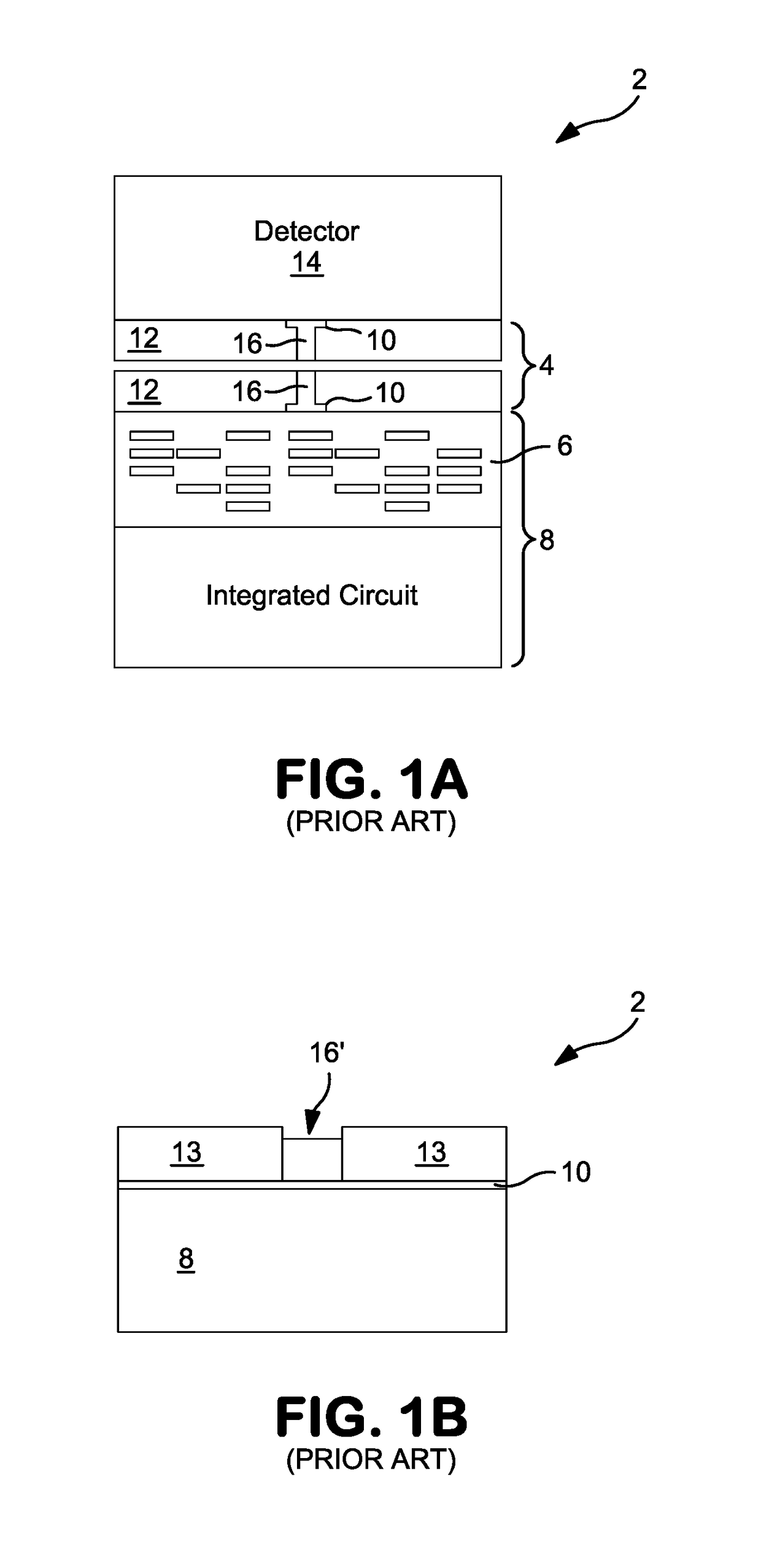
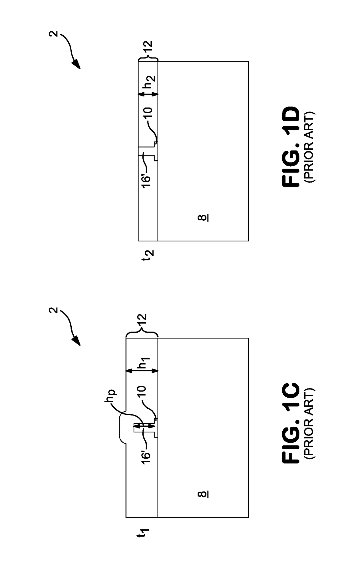
[0030]Implementations will now be described that are particularly useful in the formation of 3D stacked wafers, such as wafer 2 in FIG. 1A, which may be a SiPIN hybrid sensor. The implementations include test structures and improved in-situ (e.g., on the same wafer), direct feedback monitoring of wafer and feature depth(s) during deposition and / or thinning processes, such as, respectively, electroplating and / or chemical mechanical polishing (CMP) processes. The implementations also provide methods for determining endpoints for such processes, and for in-situ adjusting of deposition and / or thinning operating conditions. The example implementations of deposition by metal plating and thinning by CMP polishing techniques are not intended to limit the environment of the invention in any way to s...


PUM


Abstract

Systems and methods of in-situ calibration of semiconductor material layer deposition and removal processes are disclosed. Sets of test structures including one or more calibration vias or posts are used to precisely monitor processes such as plating and polishing, respectively. Known (e.g., empirically determined) relationships between the test structure features and product feature enable monitoring of wafer processing progress. Optical inspection of the calibration feature(s) during processing cycles permits dynamic operating condition adjustments and precise cessation of processing when desired product feature characteristics have been achieved.

Description

FIELD OF THE INVENTION[0001]The invention is generally related to the field of integrated circuit manufacturing, and specifically to test structures and improved in-situ direct feedback monitoring depth during wafer deposition (e.g, electroplating) and / or thinning (e.g, chemical mechanical polishing, CMP) processes, and for determining endpoints for such processes.BACKGROUND[0002]Semiconductor wafer bonding processes have been developed for bonding two silicon wafers together to form a new wafer, such as wafer 2 shown in FIG. 1A that includes a direct bond hybridization (DBH) structure 4. DBH processing may be used in the formation of a focal plane array comprised of a detector wafer 14 stacked on a read out integrated circuit (ROIC) 8, which includes analog and digital integrated circuits 6, resulting in a SiPIN hybrid sensor. Between the detector wafer 14 and the integrated circuits 6 may be found metal contact layers 10 and a metal interposer layer (e.g., interconnecting posts 16...

Claims


Application Information

Patent Timeline
Patent Type & Authority Patents(United States)
IPC IPC(8): H01L21/66B24B37/04B24B37/10B24B49/12B24B37/013H01L21/306H01L21/768H01L21/308H01L21/321
CPCH01L22/26B24B37/013B24B37/04B24B37/105B24B49/12H01L21/30625H01L21/76879H01L22/12H01L21/308H01L22/30H01L21/3212H01L21/76885H01L21/2885H01L21/76819H01L2924/14H01L2224/08145H01L24/08H01L24/80H01L2224/80894H01L2224/03845H01L2224/03462H01L24/03H01L24/05H01L2224/05655H01L2924/00012H01L2924/00014H01L24/11
Inventor KILCOYNE, SEAN P.EMERSON, ROBERT M.LIGUORI, MICHAEL V.
Owner RAYTHEON CO
Features
  • R&D
  • Intellectual Property
  • Life Sciences
  • Materials
  • Tech Scout
  • Unparalleled Data Quality
  • Higher Quality Content
  • 60% Fewer Hallucinations
Learn More