Semiconductor device
a technology of semiconductors and devices, applied in the direction of safety devices for heat exchange apparatus, indirect heat exchangers, light and heating apparatus, etc., can solve the problems of insufficient cooling from the center substrate, large thickness of the power module, and increased space size for arranging the power module, etc., to achieve efficient cooling
- Summary
- Abstract
- Description
- Claims
- Application Information
AI Technical Summary
Benefits of technology
Problems solved by technology
Method used
Image

Examples
first embodiment
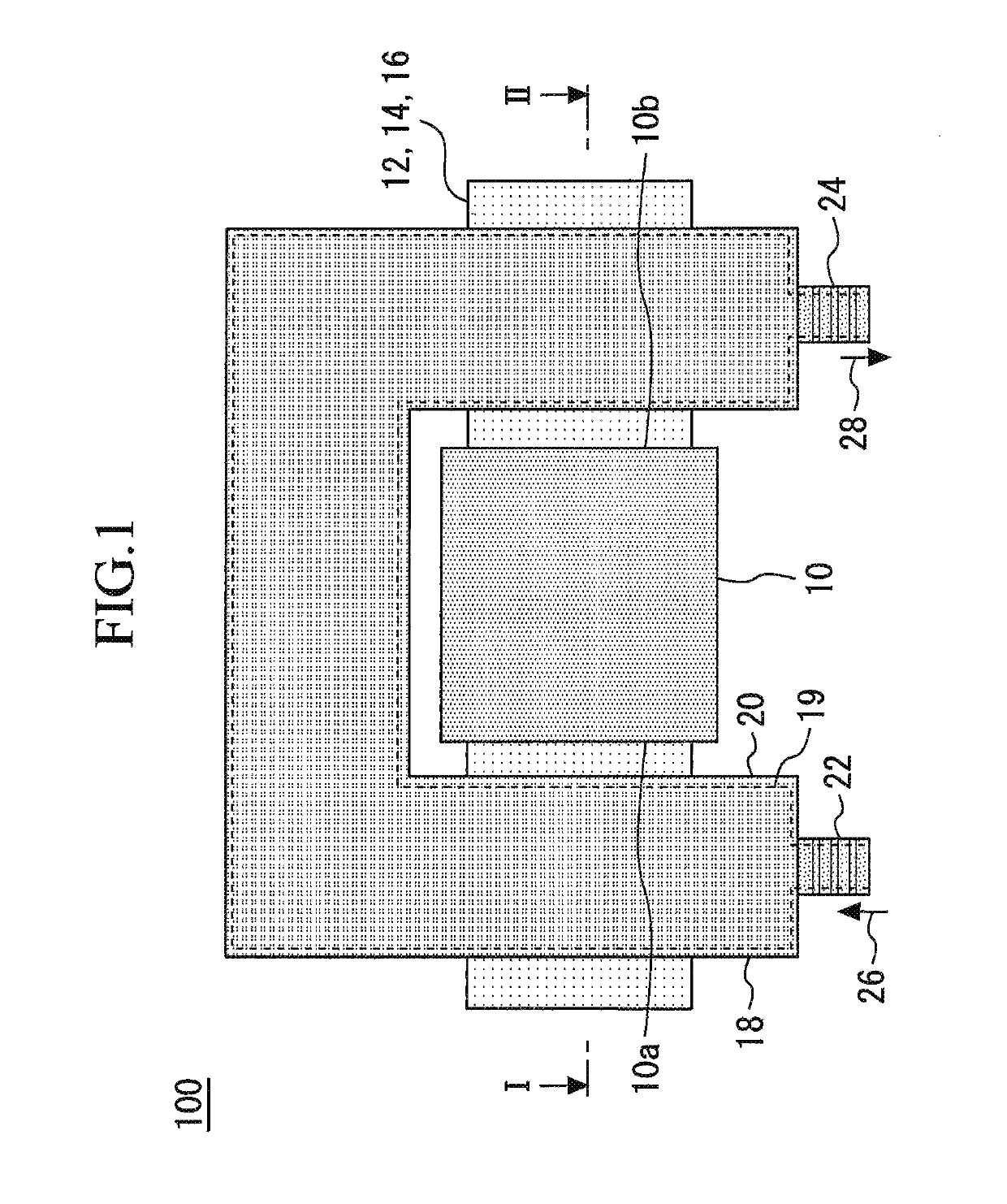
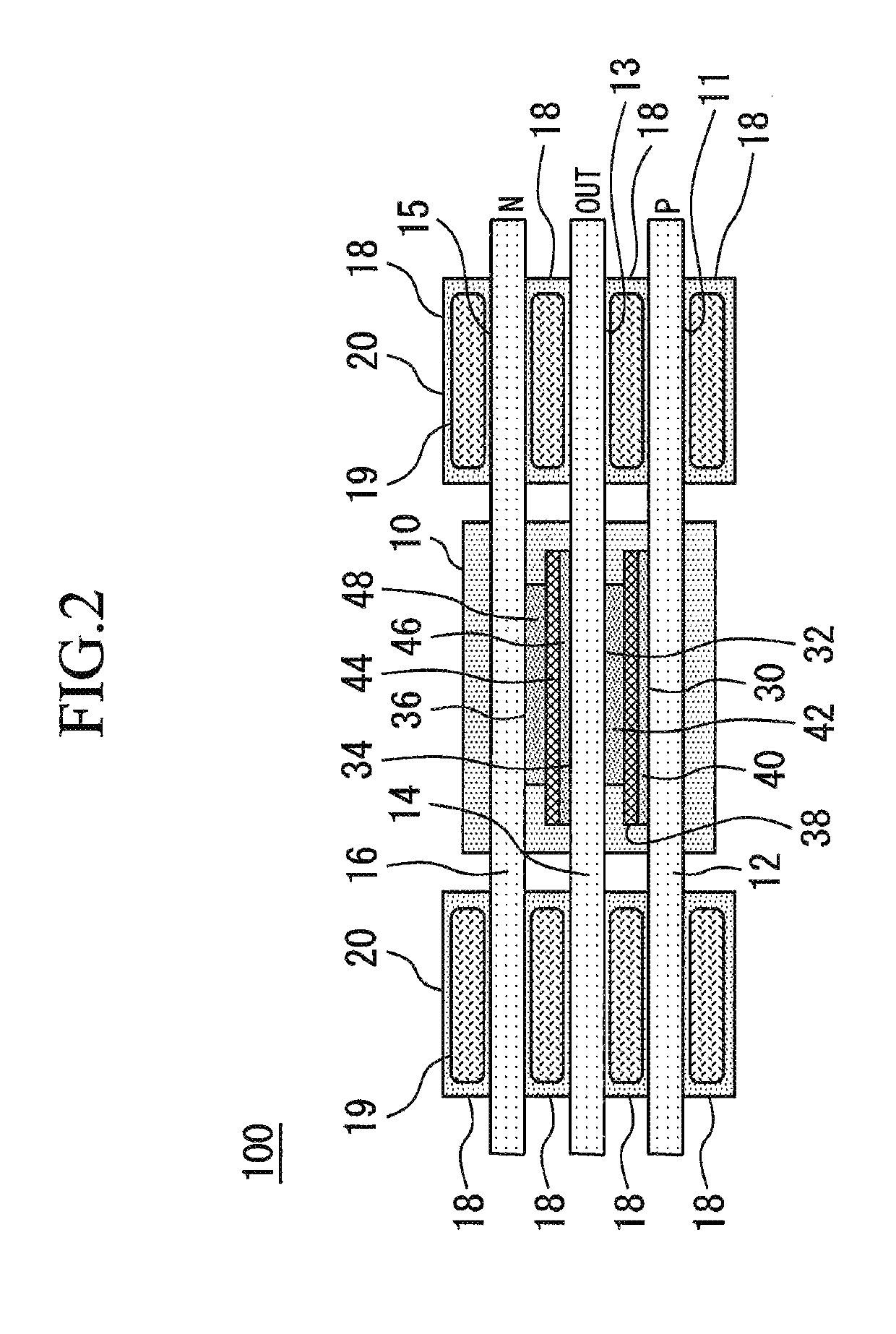
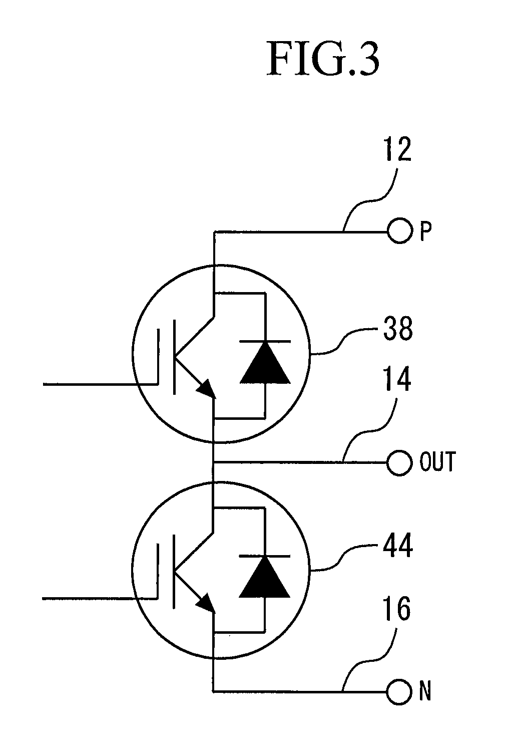
[0038]FIG. 1 is a plan view showing a semiconductor device 100 according to a first embodiment. The semiconductor device 100 has a sealing member 10. A first metal plate 12, a second metal plate 14 and a third metal plate 16 protrude from side surfaces of the sealing member 10. The first metal plate 12, the second metal plate 14 and the third metal plate 16 protrude from both sides of the sealing member 10. The first metal plate 12, the second metal plate 14 and the third metal plate 16 are laminated in this order.
[0039]The semiconductor device 100 has a cooling member 18. The cooling member 18 has a cooling flow channel 19 which is a flow passage for cooling liquid. The cooling member 18 has an insulator 20 surrounding the cooling flow channel 19. In this embodiment, the semiconductor device 100 has a plurality of cooling members 18. The plural cooling members 18 are provided so as to overlap one another in plan view. Each of the plural cooling members 18 is provided beneath the fi...
second embodiment
[0089]FIG. 14 is a plan view showing a semiconductor device 800 according to a second embodiment. In this embodiment, the structures of plural cooling members 818a, 818b are different from that of the first embodiment. Each of the plural cooling members 818a, 818b has plural heat pipes 854. One end of each heat pipe 854 is provided above or below any metal plate of the first metal plate 12, the second metal plate 14 and the third metal plate 16. The other end of each heat pipe 854 is connected to a heat sink 856.
[0090]Each heat pipe 854 has operating liquid therein. The operating liquid is vaporized by heat from the first metal plate 12, the second metal plate 14 or the third metal plate 16. The vapor of the operating liquid moves toward the heat sink 856 in the heat pipe 854. The vapor of the operating liquid is cooled to be returned to liquid on the side of the heat sink 856. Thereafter, the operating liquid moves toward the first metal plate 12, the second metal plate 14 and the ...
third embodiment
[0098]FIG. 18 is a plan view of a semiconductor device 1100 according to a third embodiment. The semiconductor device 1100 has a cooling member 1118. The cooling member 1118 has a heat sink 1162. A first metal plate 1112, a second metal plate 1114 and a third metal plate 1116 protrude from the sealing member 10. The second metal plate 1114 extends from the sealing member 10 in a direction different from the extension direction of the first metal plate 1112. The third metal plate 1116 extends from the sealing member 10 in a direction different from the extension directions of the first metal plate 1112 and the second metal plate 1114.
[0099]FIG. 19 is a cross-sectional view obtained by cutting the semiconductor device 1100 according to the third embodiment along a I-II line of FIG. 18. FIG. 20 is a cross-sectional view obtained by cutting the semiconductor device 1100 according to the third embodiment along a III-IV line of FIG. 18. The cooling member 1118 has a heat sink 1162 and an ...
PUM
| Property | Measurement | Unit |
|---|---|---|
| area | aaaaa | aaaaa |
| width | aaaaa | aaaaa |
| thermal-conductive | aaaaa | aaaaa |
Abstract
Description
Claims
Application Information
 - R&D
- Intellectual Property
- Life Sciences
- Materials
- Tech Scout
- Unparalleled Data Quality
- Higher Quality Content
- 60% Fewer Hallucinations
Browse by: Latest US Patents, China's latest patents, Technical Efficacy Thesaurus, Application Domain, Technology Topic, Popular Technical Reports.
© 2025 PatSnap. All rights reserved.Legal|Privacy policy|Modern Slavery Act Transparency Statement|Sitemap|About US| Contact US: help@patsnap.com