Organic EL display device and liquid crystal display device
a display device and liquid crystal technology, applied in non-linear optics, instruments, chemistry apparatuses and processes, etc., can solve the problems of low rigidity of flexible display devices, inconvenience in handling display devices, and resin substrates prone to plastic deformation, etc., to achieve low rigidity and sufficient flexibility
- Summary
- Abstract
- Description
- Claims
- Application Information
AI Technical Summary
Benefits of technology
Problems solved by technology
Method used
Image
Examples
embodiment 1
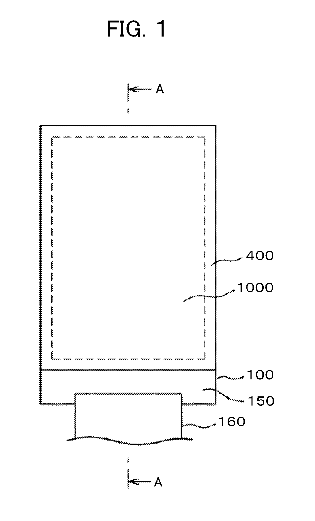
[0037]FIG. 1 is a plan view of an organic EL display device to which the invention is applied. The organic EL display device of the invention can be bent flexibly. Because organic EL display devices do not require a backlight, they are advantageous as flexible display devices. As illustrated in FIG. 1, the organic EL display device includes a display area 1000 and a terminal section 150. An anti-reflective polarizing plate 400 is glued to cover the display area 1000. A flexible wiring substrate 160 is connected to the terminal section 150 so as to supply electric power and signals to the organic EL display device.
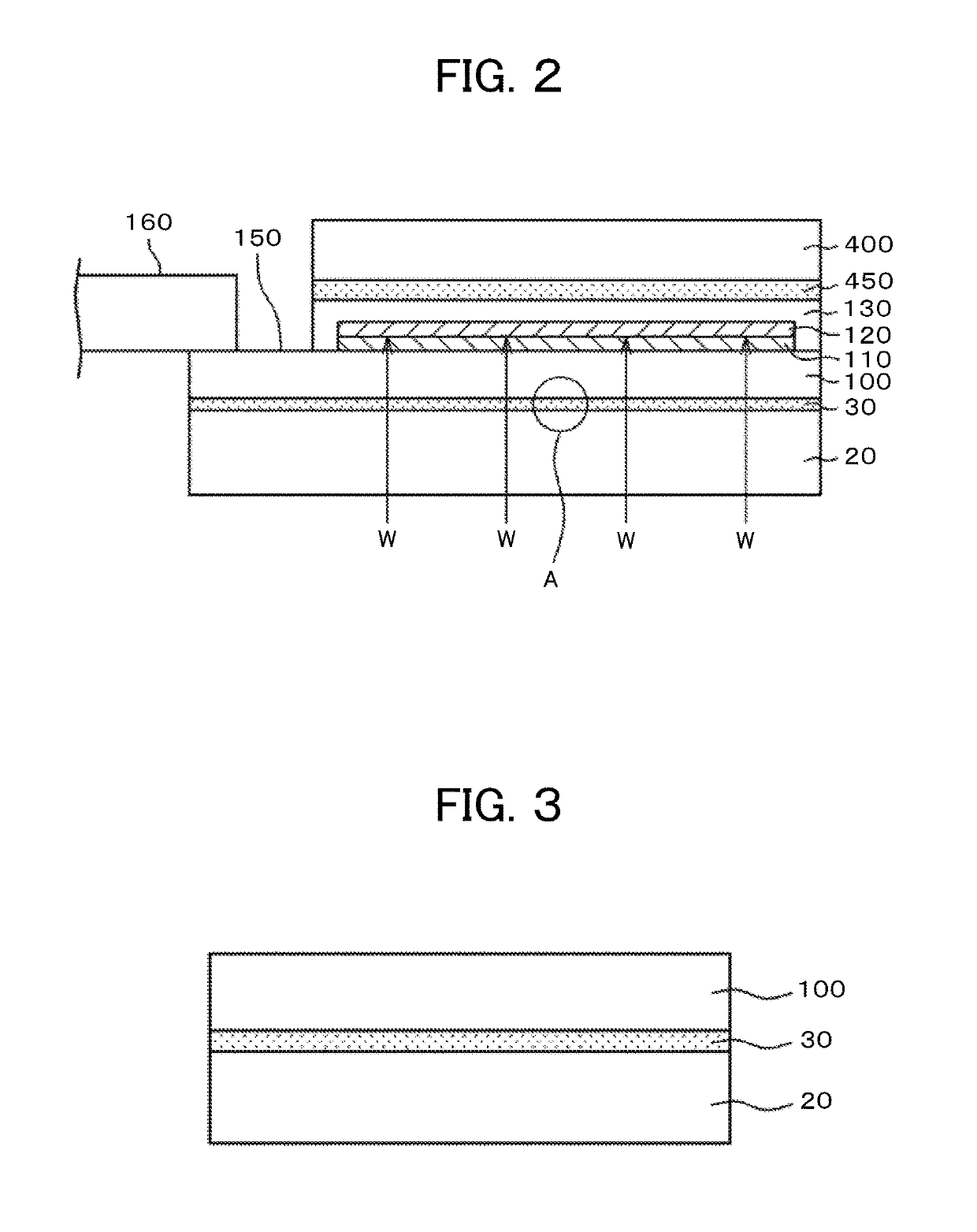
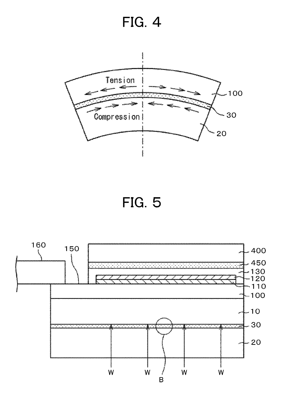
[0038]FIG. 2 is a cross section taken along line A-A of FIG. 1, presented as a comparative example. As illustrated, an array layer 110 is formed on a resin substrate 100. The array layer 110 includes thin film transistors (TFTs), video signal lines, scan lines, power lines, and so forth. The resin substrate 100 is described as a polyimide substrate because polyimide substra...
embodiment 2
[0063]Organic EL display devices can be divided into two types: those in which organic EL materials are used such that the organic EL layer emits lights of different colors for the pixels; and those in which the organic EL layer emits white light and a color filter is used to produce colored images. When the color filter is used, the counter substrate on which the color filter is formed is disposed above the organic EL layer.
[0064]FIG. 13 illustrates an example of such a case. FIG. 13 is the same as FIG. 5 related to Embodiment 1 in terms of the fabricating steps up to the formation of the protective layer 130 to cover the organic EL layer 120. As illustrated in FIG. 13, in order to glue a counter substrate 200 to the protective layer 130, a sealing material 210 is formed on the peripheral region of the protective layer 130, and a UV-curable resin 220 is applied as an adhesive to the internal region within the peripheral region. The sealing material 210 is used to prevent the UV-cur...
embodiment 3
[0071]In Embodiments 1 and 2, the array layer 110 and the organic EL layer 120 are formed on the polyimide substrate 100. By contrast, in Embodiment 3 of the invention, the array layer 110 and the organic EL layer 120 are directly formed on the glass substrate 10 without using the polyimide substrate 100. FIG. 15 is a cross section according to Embodiment 3.
[0072]As illustrated in FIG. 15, the array layer 110 and the organic EL layer 120 are formed on the glass substrate 10. The other components are the same as those of FIG. 13 related to Embodiment 2. The section D of FIG. 15, which illustrates the adhesion between the counter substrate 200 and an upper polarizing plate 410, is the same as FIG. 14 related to Embodiment 2. Also, the section E of FIG. 15, which illustrates the adhesion between the glass substrate 10 and the support substrate 20, is the same as FIG. 7 related to Embodiment 1.
[0073]If light passing through the counter substrate 200 is scattered, the image being produce...
PUM
| Property | Measurement | Unit |
|---|---|---|
| thickness | aaaaa | aaaaa |
| thick | aaaaa | aaaaa |
| thick | aaaaa | aaaaa |
Abstract
Description
Claims
Application Information


