Optical verification system and methods of verifying micro device transfer

a verification system and optical verification technology, applied in the field of micro device transfer, can solve problems such as integration and packaging problems

Active Publication Date: 2019-10-08
APPLE INC
View PDF24 Cites 6 Cited by
  • Summary
  • Abstract
  • Description
  • Claims
  • Application Information

AI Technical Summary

Problems solved by technology

Integration and packaging issues are one of the main obstacles for the commercialization of micro devices such as radio frequen

Method used


Image

  • Optical verification system and methods of verifying micro device transfer
  • Optical verification system and methods of verifying micro device transfer
  • Optical verification system and methods of verifying micro device transfer

Examples


Embodiment Construction

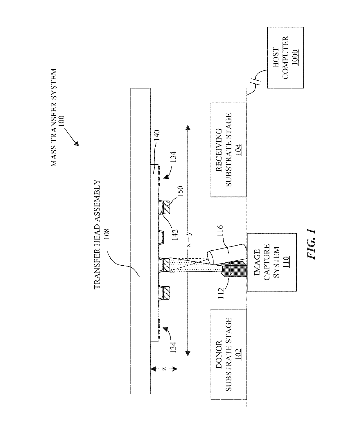
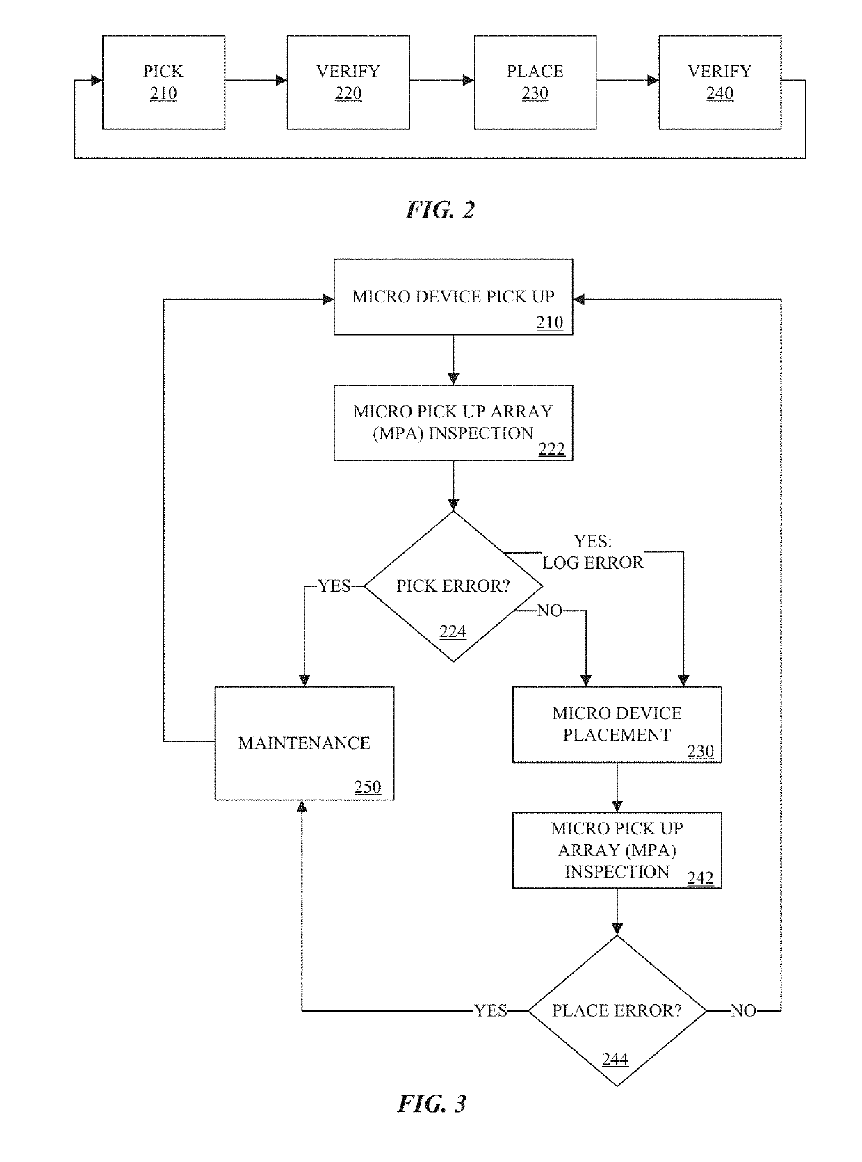
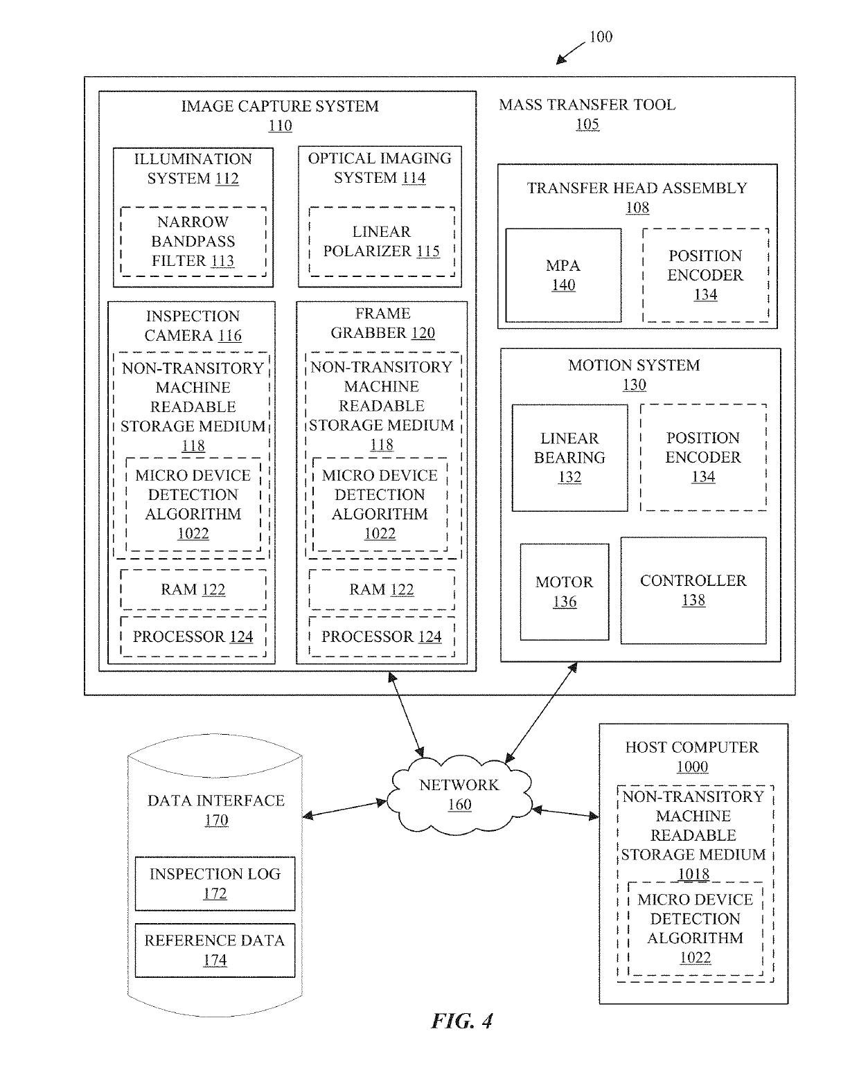
[0021]Embodiments describe systems and methods for verifying that micro devices have been picked from a donor and are poised to be placed to a receiving substrate. The methods may also be used to verify that the micro devices have been placed to a receiving substrate, and that the transfer system is poised for the next pick up operation of additional micro devices. The terms “micro” device, “micro” LED, or “micro” device transfer head as used herein may refer to the descriptive size of certain devices or structures in accordance with embodiments. As used herein, the term “micro” is meant to refer to the scale of 1 to 300 μm. For example, each micro device or transfer head may have a maximum length or width of 1 to 300 μm, 1 to 100 μm, or less. In some embodiments, the micro devices and corresponding transfer heads may each have a maximum length and width of 20 μm, 10 μm, or 5μm. However, it is to be appreciated that embodiments of the present invention are not necessarily so limited...


PUM


Abstract

An optical verification method and mass transfer system described. In an embodiments, a mass transfer sequence may be accompanied by optical imaging and inspection to detect pick and place errors. The optical imaging and inspection techniques may be performed in-situ.

Description

RELATED APPLICATIONS[0001]This application claims the benefit of priority from U.S. Provisional Application No. 62 / 393,441, filed on Sep. 12, 2016, which is herein incorporated by reference.BACKGROUNDField[0002]Embodiments relate to the transfer of micro devices. More particularly, embodiments relate to systems and methods for monitoring micro device transfer between a donor substrate and a receiving substrateBackground Information[0003]Integration and packaging issues are one of the main obstacles for the commercialization of micro devices such as radio frequency (RF) microelectromechanical systems (MEMS) microswitches, light-emitting diodes (LEDs), and MEMS or quartz-based oscillators.[0004]Traditional technologies for transferring of devices such as “direct printing” and “transfer printing” include transfer by wafer bonding from a transfer wafer to a receiving wafer. In both traditional and variations of the direct printing and transfer printing technologies, the transfer wafer i...

Claims


Application Information

Patent Timeline
IPC IPC(8): G06K9/00G06T7/00
CPCG06T7/0008G06T2207/30148G06T7/001
Inventor CZARNOTA, PATRICK J.PARKS, PAUL ARGUSLIGHT, NILE A.BATHURST, STEPHEN P.HIGGINSON, JOHN H.DEMING, STEPHEN R.MARTIN, ROBERT B.CHAN, TSAN Y.BIBL, ANDREAS
Owner APPLE INC
Why Eureka
Try Eureka