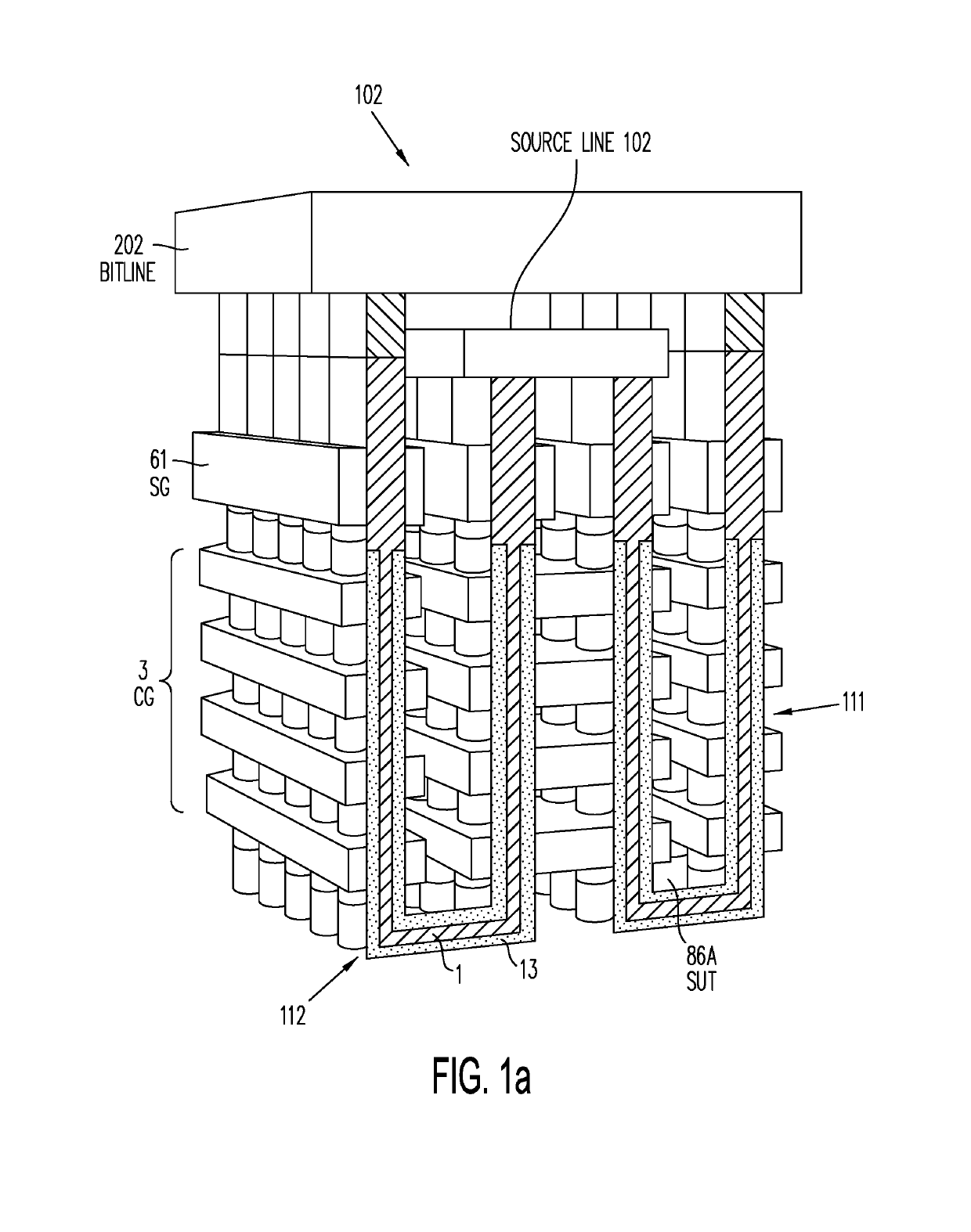
[0020]According to one embodiment of the present invention, a high-density memory structure, referred to as a three-dimensional vertical NOR Flash memory string (“multi-gate vertical NOR string,” or simply “vertical NOR string”). The vertical NOR string includes a number of thin-film transistors (“TFTs”) connected in parallel, having a shared source region and a shared drain region each extending generally in a vertical direction. In addition, the vertical NOR string includes multiple horizontal control gates each controlling a respective one of the TFTs in the vertical NOR string. As the TFTs in a vertical NOR string are connected in parallel, a read current in a vertical NOR string is conducted over a much lesser resistance than the read current through a NAND string of a comparable number of TFTs. To read or program any one of the TFTs in a vertical NOR string, only that TFT needs to be activated, all other TFTs in the vertical NOR string can remain non-conducting. Consequently, a vertical NOR string may include many more TFTs (e.g., several hundreds or more), while allowing faster sensing and minimizing program-disturb or read-disturb conditions.
[0024]According to embodiments of the present invention, variations in threshold voltages of TFTs within a vertical NOR string may be compensated by providing one or more electrically programmable reference vertical NOR strings in the same or another multi-gate vertical NOR string array. Background leakage currents inherent to a vertical NOR string can be substantially neutralized during a read operation by comparing the results of the TFT being read to that of a TFT that is concurrently read on a programmable reference vertical NOR string. In some embodiments, each TFT of a vertical NOR string is shaped so as to amplify the capacitive coupling between each control gate and its corresponding channel region thereby to enhance tunneling from the channel regions into the charge-trapping material (i.e., the storage element) during programming, and to reduce the charge injection from the control gate to the charge-trapping material during erasing. This favorable capacitive coupling is particularly useful for storing more than one bit in each TFT of a vertical NOR string. In another embodiment, the charge-trapping material of each TFT may have its structure modified to provide a high write / erase cycle endurance, albeit at a lower retention time that requires refreshing of the stored data. However, as the refreshing required of a vertical NOR string array is expected to be much less frequently than in a conventional dynamic random-access memory (DRAM), the multi-gate NOR string arrays of the present invention may operate in some DRAM applications. Such use of the vertical NOR strings allows a substantially lower cost-per-bit figure of merit, as compared to conventional DRAMs, and a substantially lower read-latency, as compared to conventional NAND string arrays.
[0026]Organizing the TFTs as vertical NOR strings—rather than the prior art vertical NAND strings—results in (i) a reduced read-latency that can approach that of a dynamic random access memory (DRAM) array, (ii) reduced sensitivities to read-disturb and program-disturb conditions that are associated with long NAND Flash strings, and (iii) reduced cost per bit, as compared to a NAND Flash string.
[0027]According to an alternative embodiment of the present invention, each active column in the memory structure includes one or more vertical NOR strings, with each NOR string having thin-film storage transistors sharing a local source line and a local bit line, the local bit line is connected by one segment of a segmented global bit line to a sense amplifier provided in the semiconductor substrate. To significantly reduce the read sense latency, rather than a global bit line that spans a substantial distance (e.g., between a half to the complete length of the chip), multiple, shorter global bit line segments are provided. Each such global segment connects one or more neighboring local bit lines through a segment connector to a segment sense amplifier provided in the semiconductor substrate. In embodiments in which the local source lines are pre-charged to a virtual ground voltage (e.g., Vss), the parasitic capacitance of the virtual ground is increased substantially by providing a short global source line segment connector which connects a group of neighboring local source lines into one local source line segment. The number of local source lines included in the segment determines the combined parasitic capacitance (C).

