Semiconductor structure and fabrication method thereof

a technology of semiconductor structure and fabrication method, which is applied in the direction of semiconductor devices, electrical devices, transistors, etc., can solve the problems of rc (resistor-capacitor) delay effect of transistors likely to increase, the performance of semiconductor structures is degraded, and the performance of semiconductor structures is poor

Active Publication Date: 2019-12-31
SEMICON MFG INT (SHANGHAI) CORP +1
View PDF4 Cites 3 Cited by
  • Summary
  • Abstract
  • Description
  • Claims
  • Application Information

AI Technical Summary

Benefits of technology

[0015]The present disclosure provides a semiconductor structure and a fabrication method of the semiconductor structure. In the disclosed embodiments, an isolation opening may be formed in the dielectric layer by removing at least a portion of a sidewall spacer. An isolation structure may be formed in the isolation opening, where the isolation structure may have a smaller dielectric constant than the sidewall spacer. A gate structure, a source-drain plug, and the isolation structure, between the gate structure and the source-drain plug, may form a source-drain capacitor. The dielectric constant of the isolation structure may be substantially small, and, thus, a capacitance value of the source-drain capacitor may be substantially small, such that a parasitic capacitance of the formed semiconductor structure may be reduced, and the performance of the semiconductor structure may be improved.
[0006]One aspect of the present disclosure includes a method for fabricating a semiconductor structure. The method includes forming a gate structure and a dielectric layer on a substrate; and forming a sidewall spacer on a sidewall surface of the gate structure. The method also includes forming a source and drain doped region in the substrate on both sides of the gate structure. The dielectric layer covers a surface of the sidewall spacer. In addition, the method includes forming a source-drain plug in the dielectric layer. The source-drain plug is connected to the source and drain doped region. Moreover, the method includes forming an isolation opening in the dielectric layer by at least partially removing the sidewall spacer. Further, the method includes forming an isolation structure in the isolation opening, wherein the isolation structure has a dielectric constant less than the sidewall spacer.
[0015]The present disclosure provides a semiconductor structure and a fabrication method of the semiconductor structure. In the disclosed embodiments, an isolation opening may be formed in the dielectric layer by removing at least a portion of a sidewall spacer. An isolation structure may be formed in the isolation opening, where the isolation structure may have a smaller dielectric constant than the sidewall spacer. A gate structure, a source-drain plug, and the isolation structure, between the gate structure and the source-drain plug, may form a source-drain capacitor. The dielectric constant of the isolation structure may be substantially small, and, thus, a capacitance value of the source-drain capacitor may be substantially small, such that a parasitic capacitance of the formed semiconductor structure may be reduced, and the performance of the semiconductor structure may be improved.
[0015]The present disclosure provides a semiconductor structure and a fabrication method of the semiconductor structure. In the disclosed embodiments, an isolation opening may be formed in the dielectric layer by removing at least a portion of a sidewall spacer. An isolation structure may be formed in the isolation opening, where the isolation structure may have a smaller dielectric constant than the sidewall spacer. A gate structure, a source-drain plug, and the isolation structure, between the gate structure and the source-drain plug, may form a source-drain capacitor. The dielectric constant of the isolation structure may be substantially small, and, thus, a capacitance value of the source-drain capacitor may be substantially small, such that a parasitic capacitance of the formed semiconductor structure may be reduced, and the performance of the semiconductor structure may be improved.
[0015]The present disclosure provides a semiconductor structure and a fabrication method of the semiconductor structure. In the disclosed embodiments, an isolation opening may be formed in the dielectric layer by removing at least a portion of a sidewall spacer. An isolation structure may be formed in the isolation opening, where the isolation structure may have a smaller dielectric constant than the sidewall spacer. A gate structure, a source-drain plug, and the isolation structure, between the gate structure and the source-drain plug, may form a source-drain capacitor. The dielectric constant of the isolation structure may be substantially small, and, thus, a capacitance value of the source-drain capacitor may be substantially small, such that a parasitic capacitance of the formed semiconductor structure may be reduced, and the performance of the semiconductor structure may be improved.

Problems solved by technology

If a capacitance value of the capacitor is large, a parasitic capacitance of the transistor is large, a RC (resistor-capacitor) delay effect of the transistor is likely to increase, and the performance of the semiconductor structure is degraded.
However, the parasitic capacitance of conventionally-formed semiconductor structures is large, and the performance of the semiconductor structure is poor and still needs to be improved.

Method used


Image

  • Semiconductor structure and fabrication method thereof
  • Semiconductor structure and fabrication method thereof
  • Semiconductor structure and fabrication method thereof

Examples


Embodiment Construction

[0012]Reference will now be made in detail to exemplary embodiments of the disclosure, which are illustrated in the accompanying drawings. Wherever possible, the same reference numbers will be used throughout the drawings to refer to the same or the alike parts.

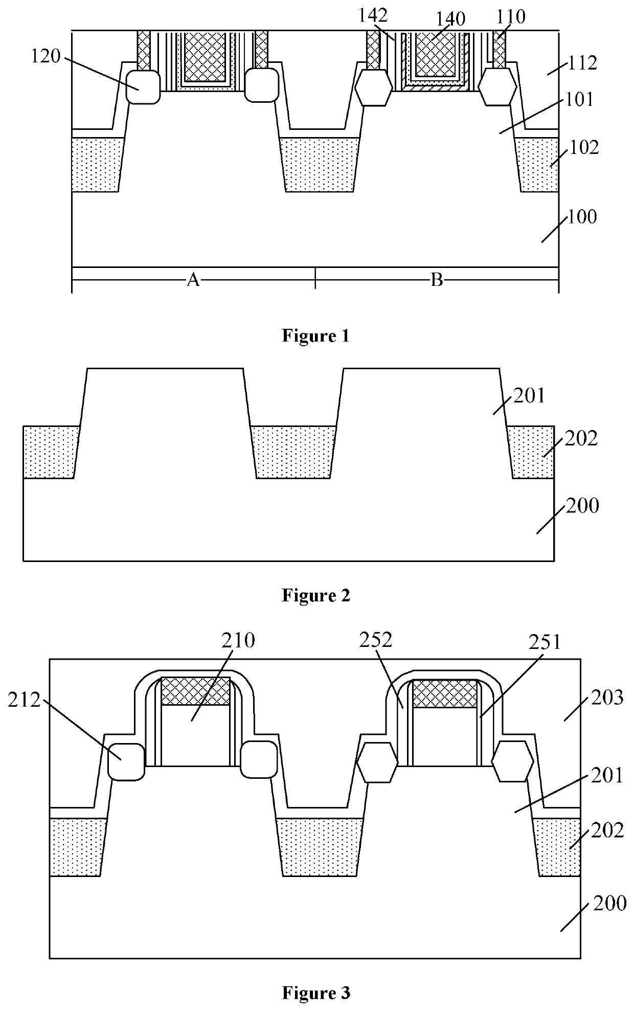
[0013]FIG. 1 illustrates a structural schematic of a semiconductor structure. Referring to FIG. 1, the semiconductor structure includes a plurality of discrete fins 101 on a substrate 100, and an isolation structure 102 on the substrate 100 between adjacent fins 101. The isolation structure 102 covers a portion of a sidewall of the fin 101. The semiconductor structure also includes a gate structure 140 across a length portion of the fin 101 and including a sidewall spacer 142 on a sidewall of the gate structure 140, and a source and drain doped layer 120 in the fin 101 on both sides of the sidewall spacer 142. Further, the semiconductor structure includes a dielectric layer 112 on the fin 101 and covering a sidewall of the si...


PUM


Abstract

A semiconductor structure and a method for fabricating the semiconductor structure are provided. The method includes forming a gate structure and a dielectric layer on a substrate; and forming a sidewall spacer on a sidewall surface of the gate structure. The method also includes forming a source and drain doped region in the substrate on both sides of the gate structure. The dielectric layer covers a surface of the sidewall spacer. In addition, the method includes forming a source-drain plug in the dielectric layer. The source-drain plug is connected to the source and drain doped region. Moreover, the method includes forming an isolation opening in the dielectric layer by at least partially removing the sidewall spacer. Further, the method includes forming an isolation structure in the isolation opening, wherein the isolation structure has a dielectric constant less than the sidewall spacer.

Description

CROSS-REFERENCES TO RELATED APPLICATIONS[0001]This application claims the priority of Chinese patent application No. 201710533393.6, filed on Jul. 3, 2017, the entirety of which is incorporated herein by reference.FIELD OF THE DISCLOSURE[0002]The present disclosure generally relates to the field of semiconductor manufacturing technology and, more particularly, relates to a semiconductor structure and fabrication method thereof.BACKGROUND[0003]With the rapid development of semiconductor manufacturing technology, semiconductor devices have been developed toward with higher component density and higher integration degree. Transistors, as the most basic semiconductor devices, have been widely used. With the increasing of the component density and the integration degree of the semiconductor devices, dimensions of a transistor are scaled down.[0004]The transistor includes: a substrate; a gate structure on the substrate; a sidewall spacer on a sidewall of the gate structure; a source and d...

Claims


Application Information

Patent Timeline
Patent Type & Authority Patents(United States)
IPC IPC(8): H01L29/417H01L29/78H01L21/311H01L29/66H01L21/02H01L29/06H01L21/768H01L29/08H01L21/764H01L27/088H01L21/8234H01L21/285H01L29/45H01L21/84H01L27/12
CPCH01L21/764H01L29/0649H01L21/0217H01L29/0847H01L21/76877H01L29/7851H01L29/41775H01L29/66545H01L27/0886H01L29/66795H01L21/31111H01L21/76802H01L29/6656H01L21/02271H01L21/0228H01L29/6653H01L21/823431H01L21/845H01L21/28568H01L21/76897H01L27/1211H01L29/45H01L29/785
Inventor ZHOU, FEI
Owner SEMICON MFG INT (SHANGHAI) CORP
Why Eureka
Try Eureka