Workpiece dividing method

a workpiece and dividing technology, applied in the direction of soldering apparatus, semiconductor/solid-state device testing/measurement, auxilary welding devices, etc., can solve the problems of workpiece damage or breakage, and achieve the effect of enhancing the divisability of the wafer

Active Publication Date: 2020-01-14
DISCO CORP
View PDF3 Cites 0 Cited by
  • Summary
  • Abstract
  • Description
  • Claims
  • Application Information

AI Technical Summary

Benefits of technology

[0004]It is therefore an object of the present invention to provide a workpiece dividing method by which a workpiece can be divided without being damaged or broken.
[0007]According to the workpiece dividing method of the present invention, in the dividing step, the pressing member is pressed against that surface of the front surface and the back surface of the workpiece at which the one end of the minute hole is not opening; therefore, the minute hole is pushed side open more easily on the diametrically enlarged one end side than on the other end side, so that dividability of the wafer is enhanced, and, accordingly, the wafer can be favorably divided without being damaged or broken.
[0008]Where the checking step of checking at which of the front surface and the back surface of the workpiece the one end or the other end of the minute hole is formed is further provided before carrying out the dividing step, it is ensured that proceeding to the dividing step can be made after grasping the one end of the minute hole on which to exert the external force by the pressing member in performing the dividing step, and, accordingly, the workpiece can be divided in a reliable manner.

Problems solved by technology

In the method disclosed in Japanese Patent Laid-Open No. 2014-221483, however, there is a problem that at the time of exerting an external force on the workpiece, the workpiece would be damaged or broken, depending on the surface against which a pressing member is pressed.

Method used


Image

  • Workpiece dividing method
  • Workpiece dividing method
  • Workpiece dividing method

Examples


first embodiment

1. First Embodiment of Dividing Method

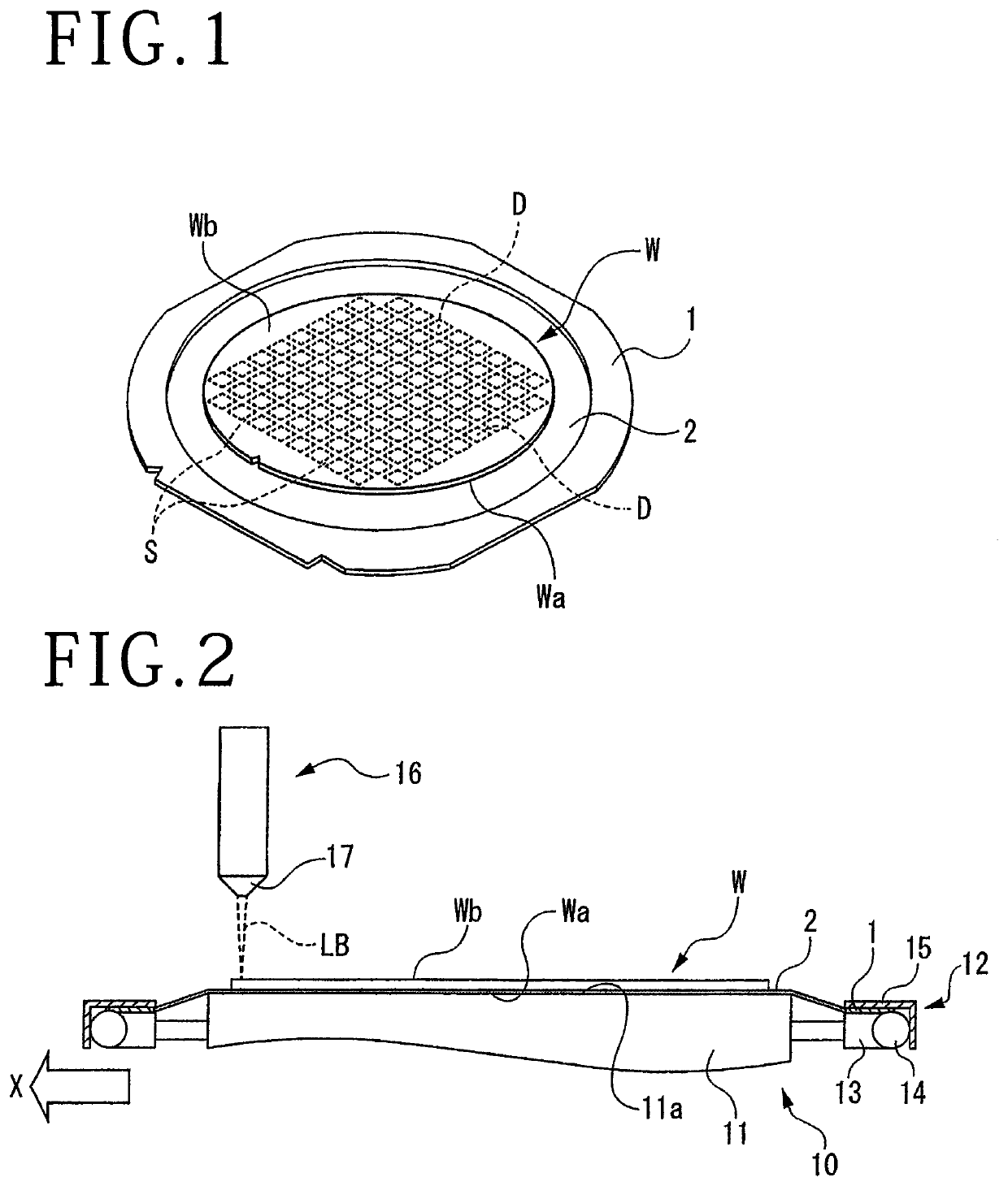
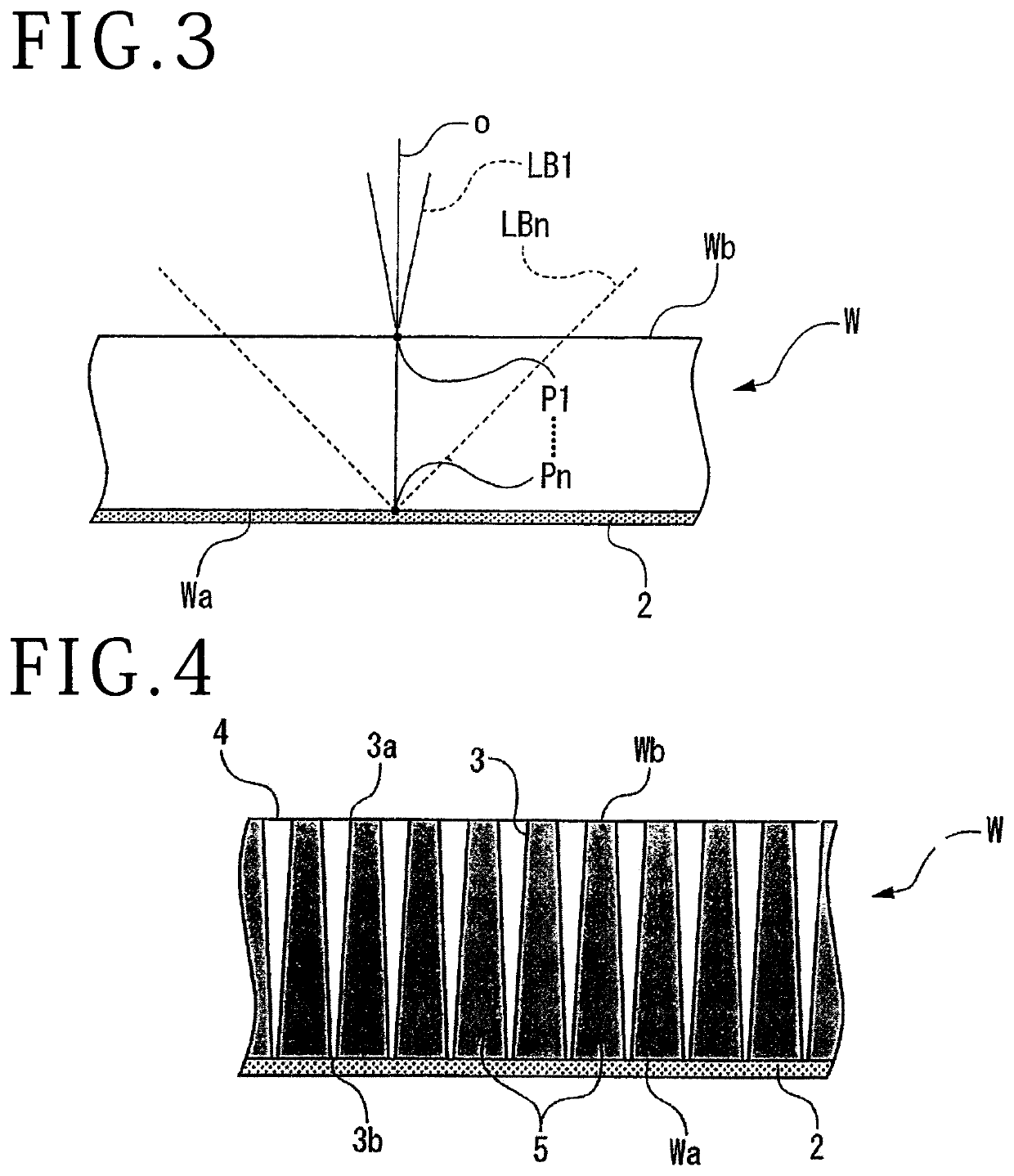
[0019]A wafer W depicted in FIG. 1 is an example of a workpiece having a circular disk-shaped substrate, and streets (division lines) S in a grid pattern are set on a front surface Wa thereof. Devices D are formed in respective regions partitioned by the streets S. On the other hand, a surface on the side opposite to the front surface Wa of the wafer W is a back surface Wb on which a laser beam is to be incident. The material of the wafer W is, for example, a glass, LT / LN (lithium tantalate / lithium niobate), SiC (silicon carbide), Si (silicon), crystal, sapphire, a ceramic or the like.

[0020]In order to divide the wafer W into chips having individual devices D, an expandable adhesive tape 2 is adhered to a lower surface of an annular frame 1 opening in the center thereof, and the front surface Wa side of the wafer W is adhered to the adhesive tape 2 exposed from the center of the frame 1, with the back surface Wb exposed to the upper side. In thi...

second embodiment

2. Second Embodiment of Dividing Method

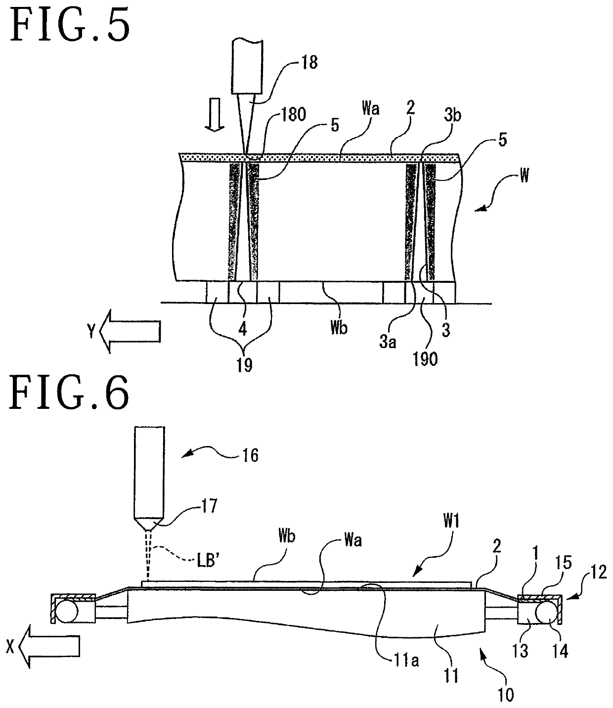
[0034]A second embodiment of the dividing method for dividing a wafer W1 into individual chips will be described below, referring to FIGS. 6 to 8.

(1) Laser Processing Step

[0035]As depicted in FIG. 6, in the similar manner to in the first embodiment, the front surface Wa side of the wafer W1 with the adhesive tape 2 adhered thereto is mounted on the holding surface 11a of the holding table 11, and the frame 1 is placed on the frame mount base 13. The clamp sections 15 are rotated around the shaft sections 14, to press and fix the upper surface of the frame 1. A laser processing step in the second embodiment is carried out, for example, under the following processing conditions 2. The wafer W1 is configured in the similar manner to the above-mentioned wafer W except for the material, and, therefore, the same reference symbols as above are used.

[Processing Conditions 2]

Material of wafer: SiC (silicon carbide)

Wavelength: 530 nm

Average output: 3 W

Re...


PUM

PropertyMeasurementUnit
refractive indexaaaaaaaaaa
diameteraaaaaaaaaa
thicknessaaaaaaaaaa

Abstract

A workpiece dividing method includes: a laser processing step of forming along each street a plurality of minute holes extending in a pulsed laser beam application direction; and a dividing step of pressing the streets by a pressing member to divide a wafer along the streets. The minute hole has one end opening at least one of a front surface and a back surface of the wafer and is decreased in diameter from the one end toward the other end. In the dividing step, the pressing member is pressed against that surface of the front surface and the back surface of the wafer at which the one end of the minute hole is not opening.

Description

BACKGROUND OF THE INVENTIONField of the Invention[0001]The present invention relates to a method of dividing a workpiece along streets (division lines) set on the workpiece.Description of the Related Art[0002]A workpiece such as a wafer has devices such as integrated circuits (ICs) and large scale integrated circuits (LSIs) formed on a front surface thereof in the state of being partitioned by streets. Examples of the method for dividing the workpiece into individual chips include a method in which a focal point of a laser beam of such a wavelength as to be transmitted through the workpiece is positioned in the inside of the workpiece at a position corresponding to the street, the laser beam and the workpiece are put into relative scanning, whereby a plurality of shield tunnels are formed inside the wafer along each street, and thereafter an external force is exerted along each street, to divide the workpiece (see, for example, Japanese Patent Laid-Open No. 2014-221483).SUMMARY OF T...

Claims


Application Information

Patent Timeline
Patent Type & Authority Patents(United States)
IPC IPC(8): H01L21/82H01L21/67B23K26/0622
CPCB23K26/0624H01L21/82H01L2221/68327H01L21/67092B23K37/0408B23K26/08B23K26/402B23K26/53B23K2103/54B23K2101/40B23K2103/50B23K2103/52B23K26/389H01L21/78H01L22/12
Inventor HATTORI, NAO
Owner DISCO CORP
Why Eureka
Try Eureka