AI technical title is built by Patsnap AI team. It summarizes the technical point description of the patent document.
a technology of single crystals and substrates, applied in the field of single crystal substrate processing, can solve problems such as poor productivity
Active Publication Date: 2018-12-18
DISCO CORP
View PDF5 Cites 0 Cited by
Summary
Abstract
Description
Claims
Application Information
AI Technical Summary
This helps you quickly interpret patents by identifying the three key elements:
Problems solved by technology
Method used
Benefits of technology
Benefits of technology
This method allows for reliable division of single-crystal substrates into individual chips without being affected by the surface film, enhancing productivity by forming shield tunnels that can be created with a single laser application, even on substrates of varying thickness.
Problems solved by technology
However, either one of the above processing methods is problematic in that the productivity is poor because in order to divide an optical device wafer made of a sapphire (Al2O3) substrate or the like along a division line, it is necessary to apply a laser beam to the same division line a plurality of times. Moreover, a single-crystal substrate where an optical device layer (film) made up of an n-type nitride semiconductor layer and a p-type nitride semiconductor layer is formed on the surface thereof requires that the single-crystal substrate be laser-processed as desired without being affected by the films.
Method used
Image
Click on the blue label to locate the original text in one second.
Reading with bidirectional positioning of images and text.
Examples
experiment 1
[Experiment 1]
[0043]Condition 1 . . . single-crystal substrate: sapphire substrate (having a thickness of 400 μm)
[0047]Condition 5 . . . the average output power of the pulsed laser beam is set to 5 W
[0048]Condition 6 . . . variable: the pulse width of the pulsed laser beam
[0049]The pulsed laser beam was applied to the sapphire substrate while the pulse width was varied from 0.1 ps to 100 ps under the above conditions, and the processed state was observed.
[0050]When the pulse width ranged from 0.1 ps to 0.6 ps, voids were formed within the sapphire substrate.
[0051]When the pulse width ranged from 0.7 ps to 63 ps, shield tunnels including fine holes and amorphous regions shielding the fine holes were formed within the sapphire substra...
experiment 2
[Experiment 2]
[0055]Condition 1 . . . single-crystal substrate: sapphire substrate (having a thickness of 400 μm)
[0056]Condition 2 . . . the wavelength of the pulsed laser beam is set to 1030 nm
[0057]Condition 3 . . . the pulse width is set to 10 ps
[0058]Condition 4 . . . the spot diameter of the pulsed laser beam is set to 10 μm
[0059]Condition 5 . . . the average output power of the pulsed laser beam is set to 5 W
[0060]Condition 6 . . . variable: the repetitive frequency of the pulsed laser beam
[0061]The pulsed laser beam was applied to the sapphire substrate while the repetitive frequency was varied from 1 kHz to 1000 kHz under the above conditions, and the processed state was observed.
[0062]When the repetitive frequency ranged from 1 kHz to 6 kHz, the inside of the sapphire substrate was broken and cracks were radially developed therein.
[0063]When the repetitive frequency ranged from 7 kHz to 640 kHz, shield tunnels including fine holes and amorphous regions shielding the fine ho...
PUM
Property
Measurement
Unit
thickness
aaaaa
aaaaa
thickness
aaaaa
aaaaa
thickness
aaaaa
aaaaa
Abstract
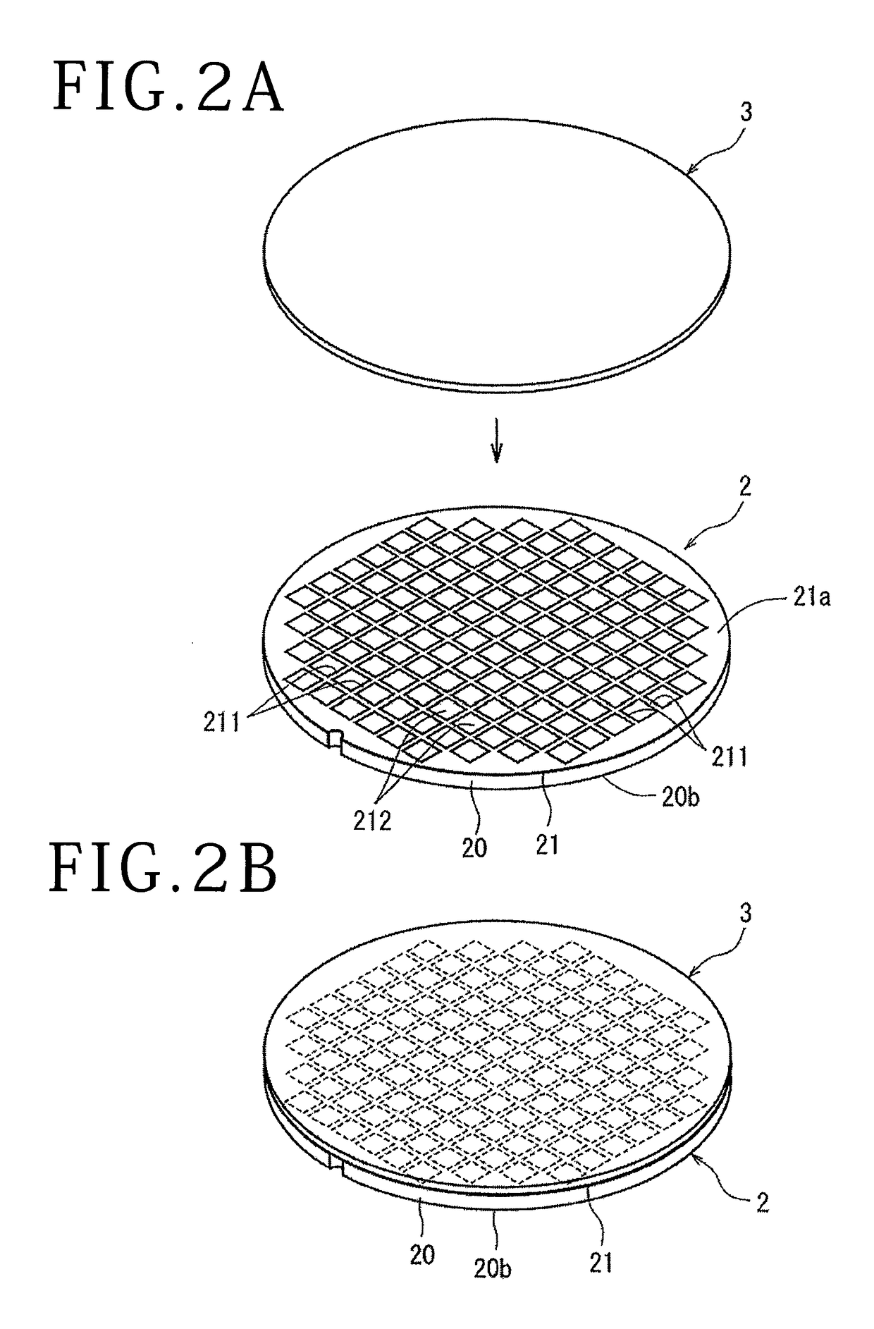
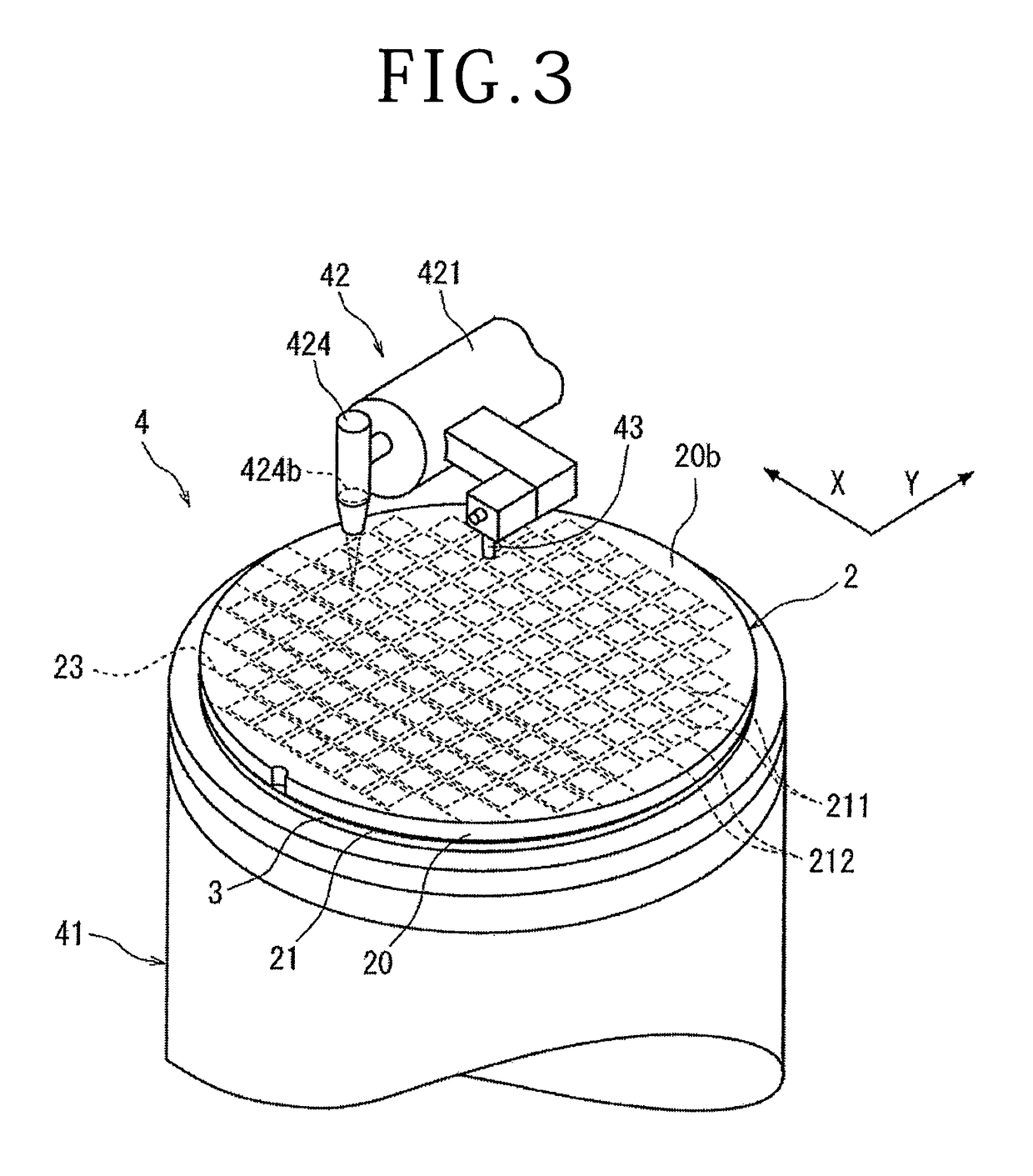
A single-crystal substrate having a film deposited on a surface thereof is processed to divide the single-crystal substrate along a plurality of preset division lines, including a shield tunnel forming step of applying a pulsed laser beam having such a wavelength that permeates through the single-crystal substrate to the single-crystal substrate from a reverse side thereof along the division lines to form shield tunnels, each including a fine hole and an amorphous region shielding the fine hole, in the single-crystal substrate along the division lines, a film removing step of removing the film deposited on the single-crystal substrate along the division lines, and a dividing step of exerting an external force on the single-crystal substrate to which the shield tunnel forming step and the film removing step are performed to divide the single-crystal substrate along the division lines along which the shield tunnels have been formed.
Description
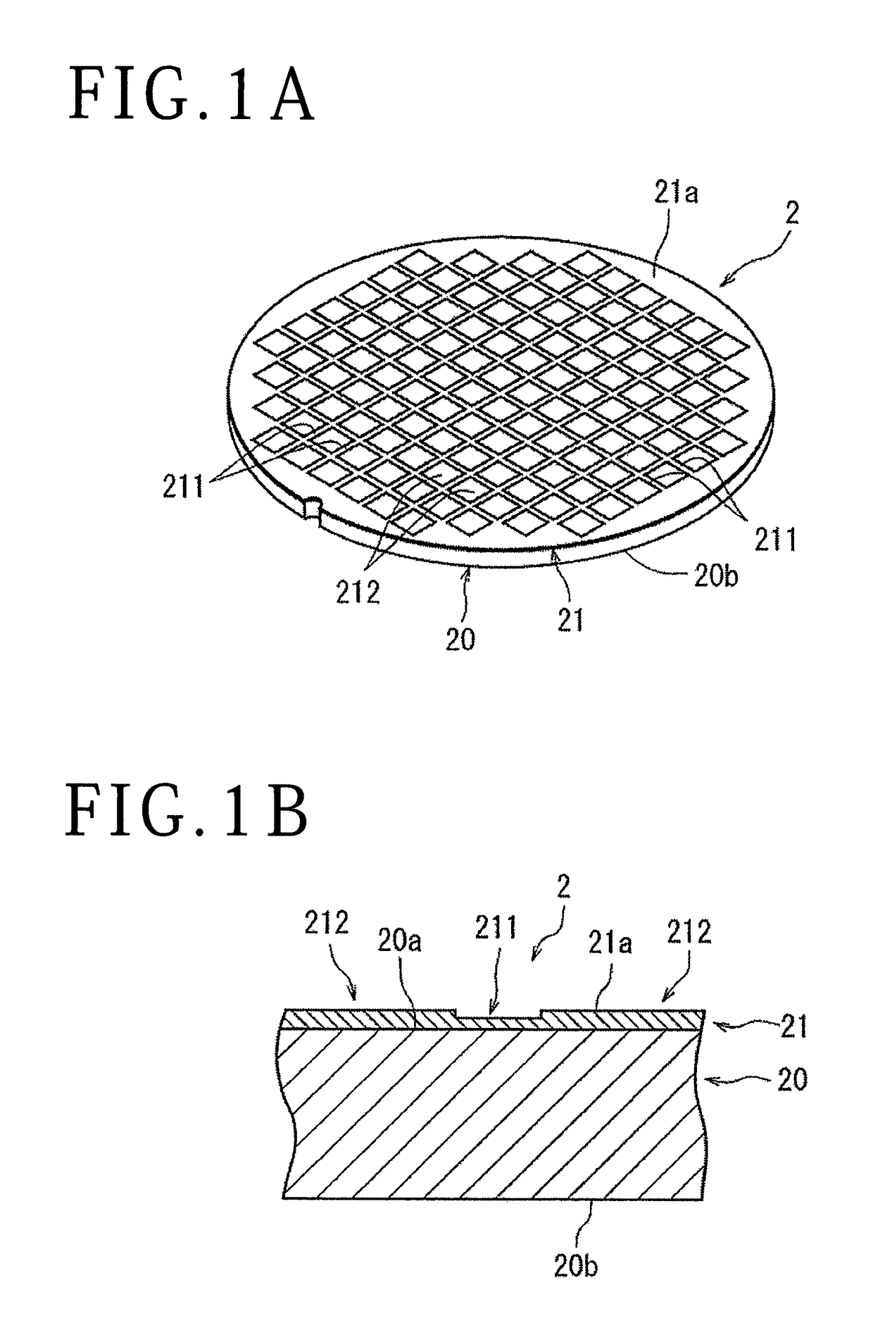
BACKGROUND OF THE INVENTION[0001]Field of the Invention[0002]The present invention relates to a method of processing a single-crystal substrate such as a sapphire (Al2O3) substrate, a siliconcarbide (SiC) substrate, a galliumnitride (GaN) substrate, a lithiumtantalate (LiTaO3) substrate, a lithium niobate (LiNbO3) substrate, a diamond substrate, a quartz substrate, or the like.[0003]Description of the Related Art[0004]In an optical device fabrication process, an optical device layer made up of an n-type nitridesemiconductor layer and a p-type nitridesemiconductor layer is stacked on the surface of a sapphire (Al2O3) substrate, a siliconcarbide (SiC) substrate, or a gallium nitride (GaN) substrate, and optical devices such as light-emitting diodes, laser diodes, or the like are formed in a plurality of regions divided by a plurality of division lines formed in a grid pattern on the optical device layer, thereby producing an optical device wafer. Then, a laser beam is applied to...
Claims
Application Information
Patent Timeline
Application Date:The date an application was filed.
Publication Date:The date a patent or application was officially published.
First Publication Date:The earliest publication date of a patent with the same application number.
Issue Date:Publication date of the patent grant document.
PCT Entry Date:The Entry date of PCT National Phase.
Estimated Expiry Date:The statutory expiry date of a patent right according to the Patent Law, and it is the longest term of protection that the patent right can achieve without the termination of the patent right due to other reasons(Term extension factor has been taken into account ).
Invalid Date:Actual expiry date is based on effective date or publication date of legal transaction data of invalid patent.

