Chip manufacturing method

a manufacturing method and chip technology, applied in the direction of manufacturing tools, solid-state devices, laser beam welding apparatus, etc., can solve the problems of processing defect and partial substrate orientation, and achieve the effect of reliably dividing the wafer, suppressing abnormal cracking, and reducing the number of times of inverting the wafer upside down

Pending Publication Date: 2022-07-28
DISCO CORP
View PDF0 Cites 0 Cited by
  • Summary
  • Abstract
  • Description
  • Claims
  • Application Information

AI Technical Summary

Benefits of technology

[0006]The present invention has been made in view of such problems. It is an object of the present invention to divide a wafer reliably by suppressing abnormal extension of cracks when dividing the wafer having a laminate on the front surface of a substrate, and reduce the number of times of inverting the wafer upside down.
[0012]The chip manufacturing method according to one aspect of the present invention performs the modified layer forming step and the grinding step in order in a state in which the back surface side is exposed, and further performs the laser-processed groove forming step in a state in which the front surface side is exposed, after the grinding step. Thus, the number of times of inversion of the wafer in a period from the modified layer forming step to the laser-processed groove forming step can be reduced to one. In addition, because the laser-processed groove forming step is performed after the modified layer forming step, abnormal extension of the crack due to a change in crystal orientation can be suppressed. It is therefore possible to reduce the number of times that the wafer is inverted upside down, and reliably divide the wafer having the laminate on the front surface of the substrate, along the planned dividing lines.

Problems solved by technology

However, when the laser-processed grooves are formed in the laminate, the front surface side of the substrate may be affected by a thermal effect of the laser beam, and consequently the crystal orientation of a partial region of the substrate which region is in proximity to a bottom portion of a processed groove may change.
Thus, when a change in the crystal orientation occurs, the cracks appear on the front surface of the substrate in such a manner as to avoid the laser-processed grooves, so that the wafer is not divided along the streets (that is, a processing defect occurs).

Method used


Image

  • Chip manufacturing method
  • Chip manufacturing method
  • Chip manufacturing method

Examples


first embodiment

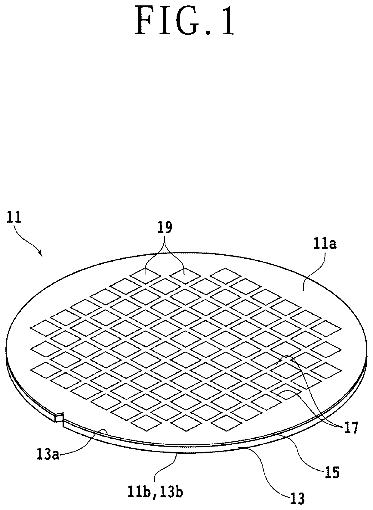
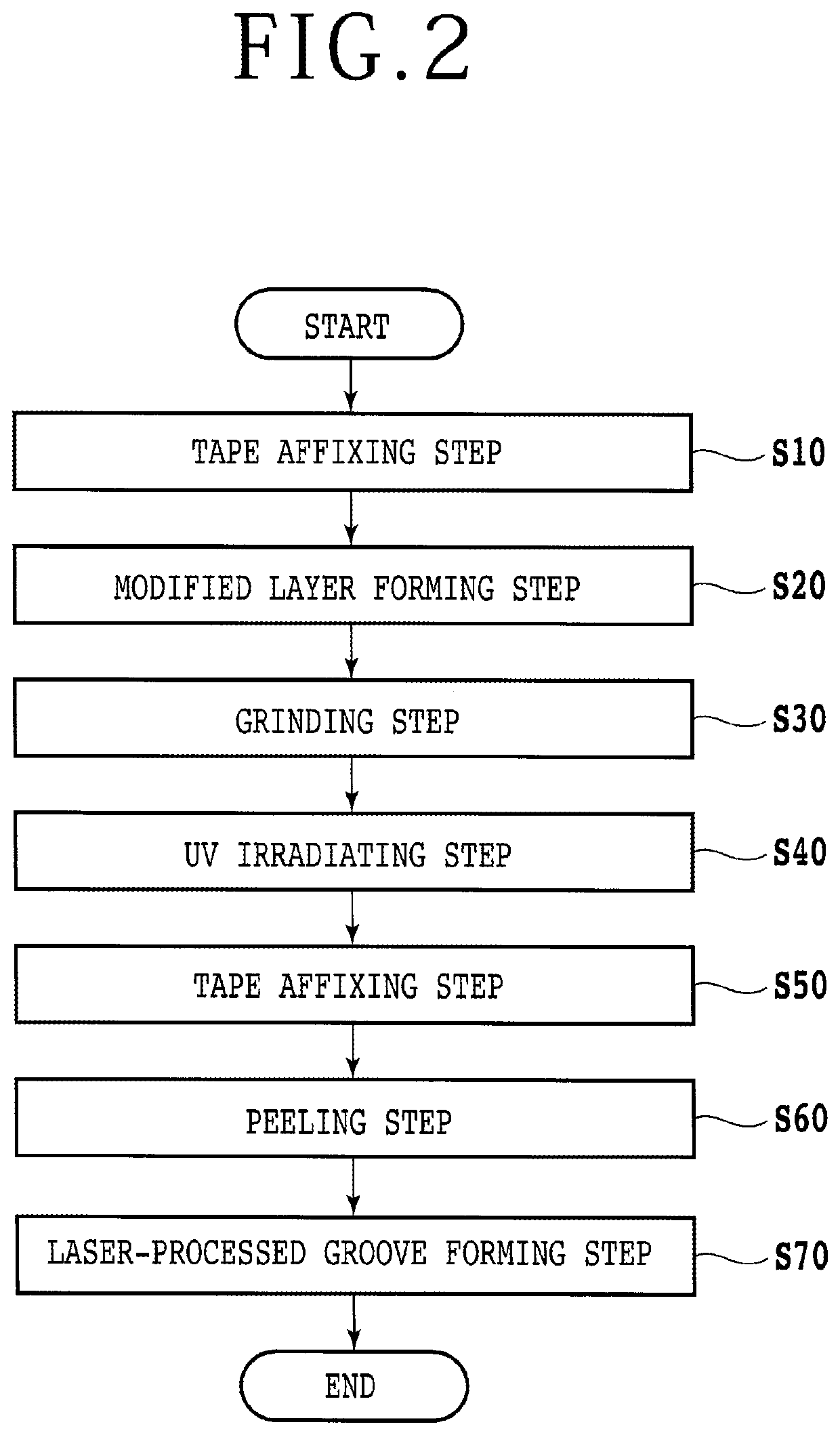
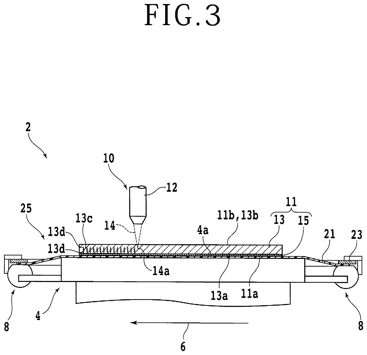
[0037]Description will next be made of a method of manufacturing a plurality of device chips (chips) 35 (see FIG. 9A and the like) by dividing the wafer 11 into units of the devices 19. FIG. 2 is a flowchart of a method of manufacturing the device chips 35 according to a First, a first protective tape 21 is affixed to the laminate 15 side of the wafer 11 (that is, a front surface 11a of the wafer 11) and one surface of an annular frame 23 (see FIG. 3) made of metal which annular frame has an opening portion of a diameter larger than that of the wafer 11 (tape affixing step S10).

[0038]In the present example, a wafer unit 25 is formed in which the wafer 11 is thus supported by the annular frame 23 via the first protective tape 21. However, the annular frame 23 is not essential. The first protective tape 21 having substantially the same diameter as that of the wafer 11 may be affixed to the front surface 11a side. The first protective tape 21 is, for example, a resin-made film in whic...

second embodiment

[0082](Second Embodiment) A second embodiment will next be described. FIG. 12 is a flowchart of a method of manufacturing device chips 35 according to the As depicted in FIG. 13, the laser-processed groove forming step S70 according to the second embodiment forms a laser-processed groove 15a4 having a predetermined depth such that the laminate 15 is not severed completely. FIG. 13 is an enlarged sectional view of the wafer 11, the enlarged sectional view depicting one laser-processed groove 15a4 not reaching the front surface 13a of the substrate 13. The laser-processed groove 15a4 can be formed by, for example, decreasing average power and repetition frequency, increasing processing feed speed, or changing the height position of the condensing point 50a. Damage to the front surface 13a side of the substrate 13 in the laser-processed groove forming step S70 can be reduced by forming the laser-processed groove 15a4 not reaching the front surface 13a.

[0083]In the second embodiment, ...


PUM


Abstract

A chip manufacturing method includes a modified layer forming step of forming a modified layer and a crack by applying, along planned dividing lines, a first laser beam having a wavelength transmitted through a substrate of a wafer including the substrate and a laminate in a state in which the back surface side of the substrate is exposed and a condensing point of the first laser beam is positioned within the substrate from the back surface side of the substrate, a grinding step of thinning the wafer to a predetermined thickness by grinding the back surface side of the substrate exposed in the modified layer forming step, and a laser-processed groove forming step of forming a laser-processed groove in the laminate by applying, along the planned dividing lines, a second laser beam having a wavelength absorbed by the substrate, from the front surface side of the wafer.

Description

BACKGROUND OF THE INVENTIONField of the Invention[0001]The present invention relates to a chip manufacturing method for manufacturing chips by dividing a wafer in which a substrate and a laminate are laminated.Description of the Related Art[0002]Semiconductor chips are generally manufactured by dividing a wafer along streets (planned dividing lines) set on a front surface of a substrate, the wafer including the substrate formed of a semiconductor such as silicon (Si) and a laminate of a Low-k film and a conductive layer or the like formed on the front surface of the substrate. Incidentally, a test element group (TEG) may be formed in partial regions of the laminate which regions are on the streets. In order to divide the wafer along the streets, laser-processed grooves are first formed along the streets by, for example, applying, along the streets, a pulsed laser beam having a wavelength absorbed by the substrate and the laminate. In the laser-processed grooves, the laminate is part...

Claims


Application Information

Patent Timeline
Patent Type & Authority Applications(United States)
IPC IPC(8): H01L21/78H01L21/268H01L21/304
CPCH01L21/78H01L21/3043H01L21/268H01L21/2683B23K26/364H01L21/6836H01L2221/68327H01L2221/6834H01L2221/68336H01L21/304
Inventor HASHIMOTO, KAZUKI
Owner DISCO CORP
Why Eureka
Try Eureka