Package substrate processing method

a packaging substrate and processing method technology, applied in the direction of grinding/polishing apparatus, grinding machines, manufacturing tools, etc., can solve the problems of affecting the quality of the finished product, the scattering of package devices in the dividing of the package substrate, and the partial leakage of the suction force applied to the package devi

Active Publication Date: 2015-05-05
DISCO CORP
View PDF8 Cites 0 Cited by
  • Summary
  • Abstract
  • Description
  • Claims
  • Application Information

AI Technical Summary

Benefits of technology

[0009]It is therefore an object of the present invention to provide a package substrate processing method which can divide the package substrate into the individual package devices without scattering of the package devices in the condition where the package devices of the package substrate are individually reliably held under suction.
[0011]As described above, the package substrate processing method according to the present invention includes the internal stress relieving step of cutting the electrode plate of the package substrate along a selected one of the division lines to form a relief groove, thereby relieving an internal stress in the package substrate, the resin layer planarizing step of grinding the synthetic resin layer of the package substrate to thereby planarize the synthetic resin layer, the package substrate holding step of holding the synthetic resin layer of the package substrate on a holding table under suction, this holding table having a plurality of crossing grooves respectively corresponding to the division lines and a plurality of suction holes respectively formed in a plurality of regions partitioned by these crossing grooves, and the package substrate dividing step of dividing the package substrate held on the holding table under suction along the division lines. Accordingly, in performing the package substrate dividing step, the plural package devices of the package substrate are reliably held under suction by the vacuum applied to the plural suction holes formed in the holding table, respectively. As a result, the package substrate can be reliably divided into the individual package devices along the division lines without scattering the package devices.

Problems solved by technology

In the case of holding the package substrate divided into the large parts to such an extent that the warp is dispersed on the jig or holding table capable of individually holding the package devices (chip size packages) under suction in the condition where the resin layer of the package substrate is in contact with the jig or holding table, there is a problem such that a suction force applied to each package device may partially leak with a decrease in size of each package device as 3 mm square or 2 mm square, causing scattering of the package devices in dividing the package substrate.

Method used


Image

  • Package substrate processing method
  • Package substrate processing method
  • Package substrate processing method

Examples


Embodiment Construction

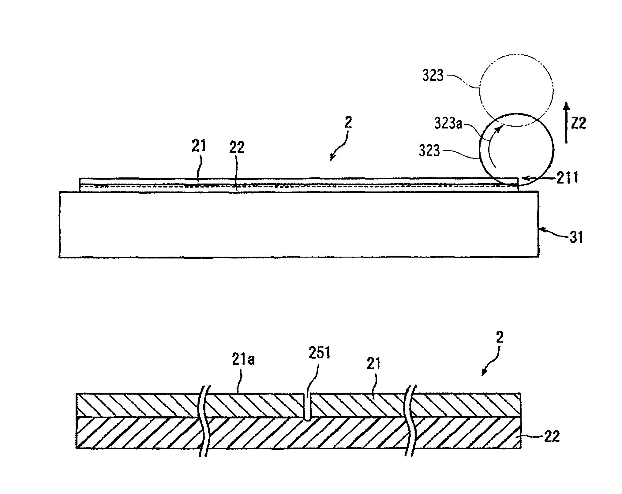
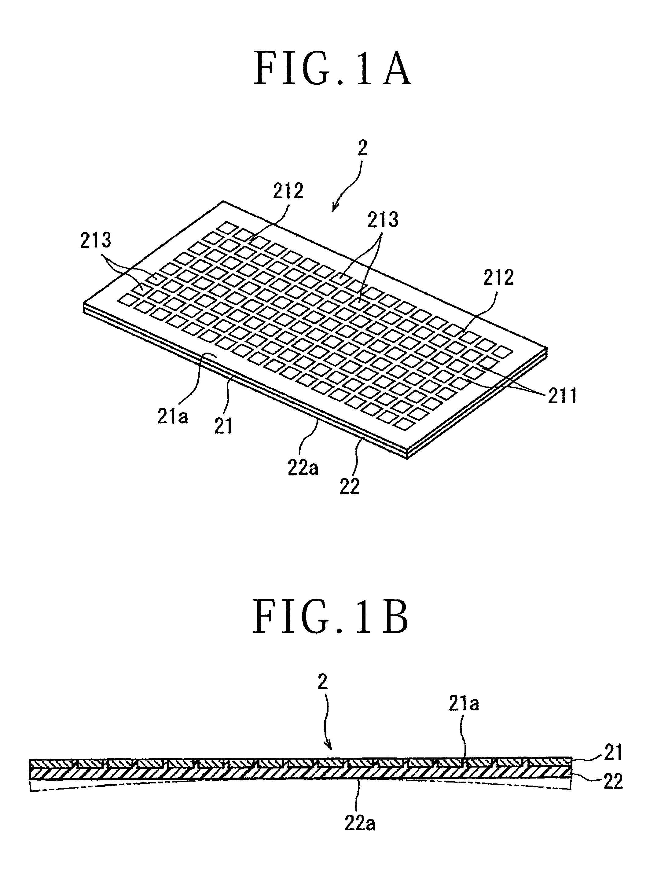
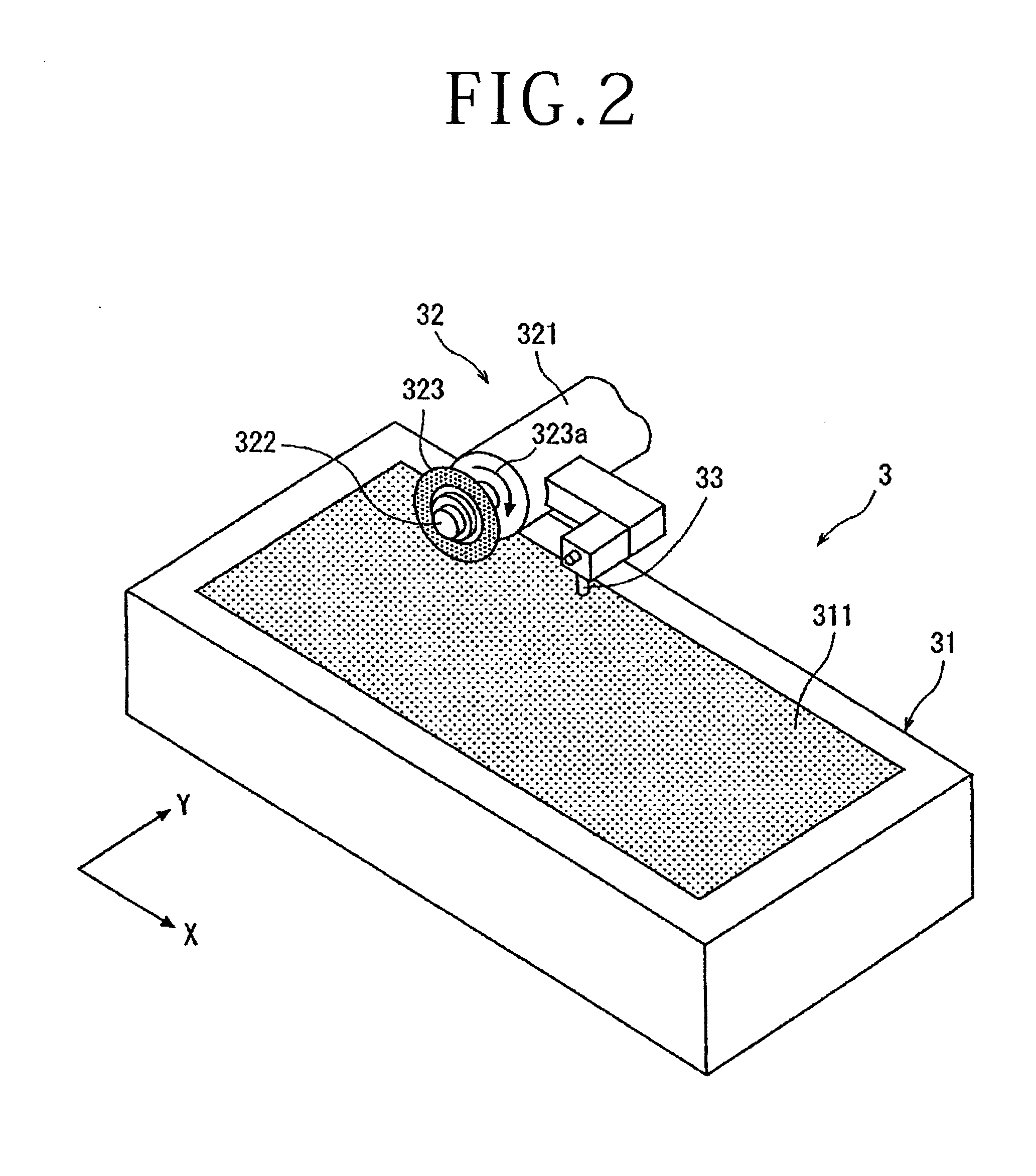
[0024]A preferred embodiment of the package substrate processing method according to the present invention will now be described in detail with reference to the attached drawings. FIG. 1A is a perspective view of a package substrate 2 as a workpiece, and FIG. 1B is a sectional view of the package substrate 2 shown in FIG. 1A. The package substrate 2 includes an electrode plate 21. A plurality of first division lines 211 extending in a first direction and a plurality of second division lines 212 extending in a second direction perpendicular to the first direction are formed on the front side 21a of the electrode plate 21. That is, the first division lines 211 intersect the second division lines 212 at right angles on the front side 21a of the electrode plate 21, thereby partitioning a plurality of rectangular regions where a plurality of package devices 213 are respectively provided. These package devices 213 are molded with a synthetic resin layer 22 from the back side of the electr...


PUM

PropertyMeasurementUnit
internal stressaaaaaaaaaa
sizeaaaaaaaaaa
weightaaaaaaaaaa

Abstract

A package substrate processing method of dividing a package substrate into a plurality of individual package devices along a plurality of division lines, the package substrate being composed of an electrode plate and a synthetic resin layer formed on the back side of the electrode plate for molding the package devices. The package substrate processing method includes an internal stress relieving step of cutting the electrode plate of the package substrate along a selected one of the division lines to form a relief groove, thereby relieving an internal stress in the package substrate, a resin layer planarizing step of grinding the synthetic resin layer of the package substrate to thereby planarize the synthetic resin layer, and a package substrate dividing step of dividing the package substrate held on a holding table under suction along the division lines.

Description

BACKGROUND OF THE INVENTION[0001]1. Field of the Invention[0002]The present invention relates to a package substrate processing method of dividing a package substrate into a plurality of individual package devices along a plurality of crossing division lines, the package substrate being composed of an electrode plate having the division lines formed on the front side for partitioning a plurality of regions where the package devices are respectively provided and a synthetic resin layer formed on the back side of the electrode plate for molding the package devices.[0003]2. Description of the Related Art[0004]In a semiconductor device fabrication process, a plurality of crossing division lines are formed on the front side of a substantially disk-shaped semiconductor wafer to thereby partition a plurality of regions where a plurality of devices such as ICs and LSIs are respectively formed. The semiconductor wafer is cut along the division lines to thereby obtain the individual devices. ...

Claims


Application Information

Patent Timeline
Patent Type & Authority Patents(United States)
IPC IPC(8): H01L21/00B24B7/22B24B41/06B28D5/00B28D5/02H01L21/304H01L21/78
CPCH01L21/78B28D5/0094B28D5/022H01L21/304B24B41/061B24B7/228H01L2224/97
Inventor SEKIYA, KAZUMA
Owner DISCO CORP
Why Eureka
Try Eureka