
Method for reducing thin films on low temperature substrates

a low-temperature substrate and thin film technology, applied in metal-working apparatus, printing, metallic material coating process, etc., can solve the problems of preventing the use of inexpensive substrates, high cost of conductive traces, and limited sintering

Active Publication Date: 2020-01-14
NCC NANO LLC
View PDF2 Cites 1 Cited by
  • Summary
  • Abstract
  • Description
  • Claims
  • Application Information

AI Technical Summary

Problems solved by technology

These two qualities, coupled with the fact that silver is the most electrically conductive metal often outweigh its high cost when making conductive traces.
Such high-temperature requirement prevents the usage of inexpensive substrates such as paper or plastic.
At low temperatures, sintering is very limited, and thus the film resistivity becomes high.
Furthermore, the need for an inert or reducing atmosphere also dramatically increases processing cost.

Method used


Image

  • Method for reducing thin films on low temperature substrates

Examples


example 1

Acid Reducer

[0039]A copper oxide dispersion was produced by mixing 3.0 g<50 nm copper (II) oxide, 3.6 g deionized water, 0.15 g PVP K-30, 0.3 g ethylene glycol, 0.04 g Tergitol® TMN-6, 0.02 g Dynol® 604, 0.02 g BYK®-020, and 0.66 g ascorbic acid in a 20 mL vial. 5 g of zirconium oxide milling media was added and the vial was agitated for 60 minutes.

[0040]The dispersion was applied to a sheet of Melinex® ST505 PET by drawdown using a #5 Meyer bar.

[0041]The sample was cured with a pulse length of 1,000 microseconds, and overlap factor of 2 at 24 feet per minute in an air environment. Although the film was not electrically conductive, the color of the film changed from dark brown to a copper color indicating significant conversion of the copper oxide to copper.

example 2

Glycol / Glycerol Reducer

[0042]A copper oxide dispersion was produced by mixing 2.0 g NanoArc® copper oxide, 5.7 g deionized water, 0.10 g PVP K-30, 0.6 g ethylene glycol, 0.03 g Tergitol® TMN-6, 0.01 g Dynol® 604, and 0.32 g glycerol in a 20 mL vial. 5 g of zirconium oxide milling media was added and the vial was agitated for 60 minutes.

[0043]The dispersion was applied to a sheet of Melinex® ST505 PET by drawdown using a #5 Meyer bar.

[0044]The sample was cured with a pulse length of 850 microseconds, and overlap factor of 2 at 24 feet per minute in an air environment. Although the film was not electrically conductive, the color of the film changed from dark brown to a copper color indicating significant conversion of the copper oxide to copper.

example 3

Glycol / Glycerol Reducer

[0045]A copper oxide dispersion was produced by mixing 2.0 g NanoArc® copper oxide, 5.4 g deionized water, 0.10 g PVP K-30, 0.6 g ethylene glycol, 0.03 g Tergitol® TMN-6, 0.01 g Dynol® 604, and 0.67 g glycerol in a 20 mL vial. 5 g of zirconium oxide milling media was added and the vial was agitated for 60 minutes.

[0046]The dispersion was applied to a sheet of Melinex® ST505 PET by drawdown using a #5 Meyer bar.

[0047]The sample was cured with a pulse length of 1,000 microseconds, and overlap factor of 3 at 24 feet per minute in an air environment. Although the film was not electrically conductive, the color of the film changed from lark brown to a copper color indicating significant conversion of the copper oxide to copper.


PUM

PropertyMeasurementUnit
temperatureaaaaaaaaaa
thickaaaaaaaaaa
speedsaaaaaaaaaa

Abstract

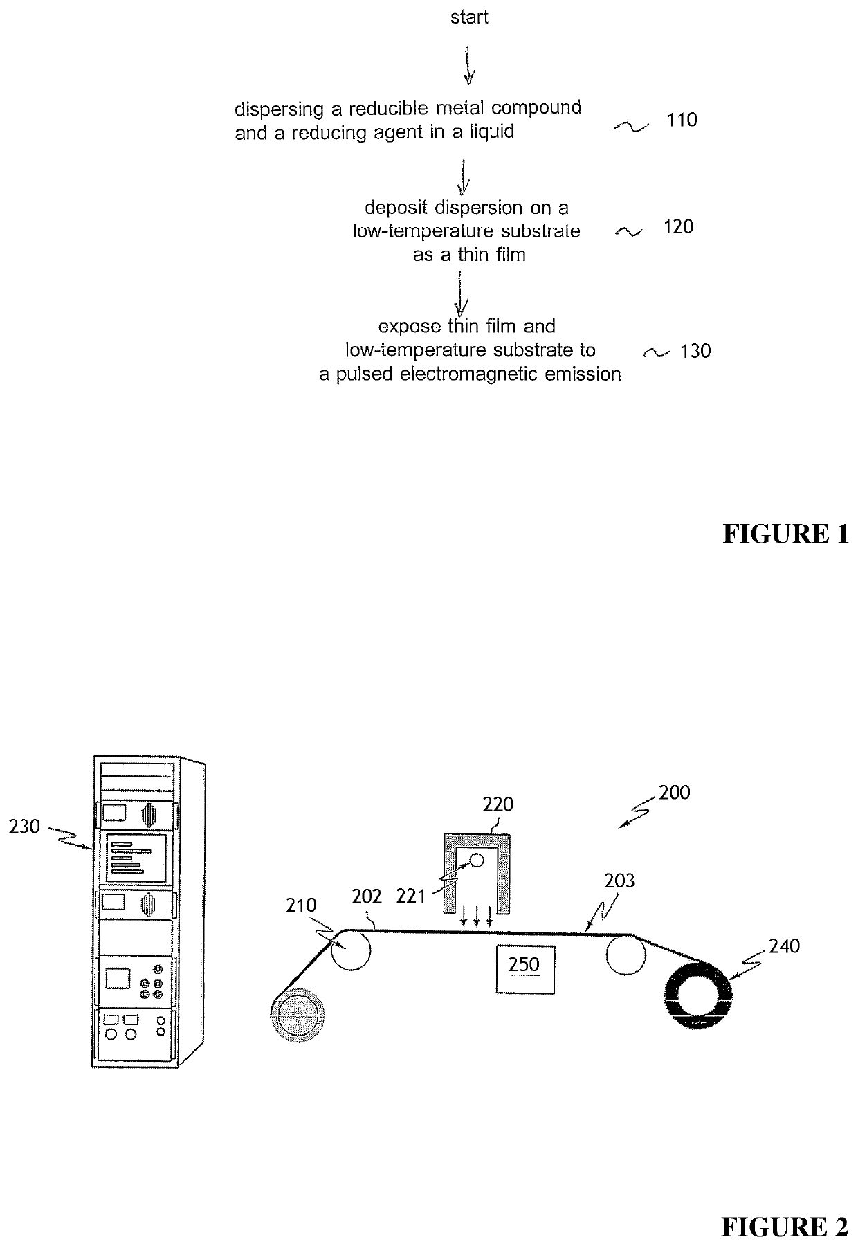
A method for producing an electrically conductive thin film on a substrate is disclosed. Initially, a reducible metal compound and a reducing agent are dispersed in a liquid. The dispersion is then deposited on a substrate as a thin film. The thin film along with the substrate is subsequently exposed to a pulsed electromagnetic emission to chemically react with the reducible metal compound and the reducing agent such that the thin film becomes electrically conductive.

Description

RELATED APPLICATIONS[0001]The present application is a divisional application of U.S. Ser. No. 14 / 582,873, filed on Dec. 24, 2014.[0002]The present application is related to U.S. Ser. No. 61 / 196,531, filed on Oct. 17, 2008, entitled “Method and Apparatus for Reacting Thin Films on Low Temperature Substrates at High Speeds,” which is incorporated herein by reference.BACKGROUND OF THE INVENTION1. Technical Field[0003]The present invention relates to curing method in general, and, in particular, to a method for reducing thin filing on low-temperature substrates.2. Description of Related Art[0004]One approach to making electronic circuits is to print electrical conductors with metallic ink onto a substrate, and the substrate is then heated to sinter the particles of the metallic ink in order to form electrical conducting traces. Generally, most printed metals suitable for electrically conduction need to be heated to a very high temperature, often within a couple hundred degrees centigra...

Claims


Application Information

Patent Timeline
Patent Type & Authority Patents(United States)
IPC IPC(8): C23C18/14H05K3/10C23C18/40C09D7/61C09D1/00B22F9/24B22F3/105C23C30/00C09D1/04B29C35/08D21H19/02B22F1/00B22F3/10C23C18/31B41M3/00C23C18/16B41M7/00H05K3/12B41M5/00B29C35/10H05K1/03B22F1/0545B22F1/103
CPCB41M7/0081H05K3/105C09D7/61H05K3/1283B41M3/006D21H19/02B22F1/0022C23C18/1692C23C18/40B22F9/24C09D1/00C23C18/1667C23C18/14C23C18/31C09D1/04B22F3/105H05K3/12B22F3/10B41M3/001C23C30/00B29C35/0805C23C18/1658B41M5/0035B41M5/0064H05K2203/10B22F2001/0033B22F2001/0066B41M5/0047H05K2203/1131H05K1/0386B29C35/10B41M7/0072H05K2203/102H05K2203/107H05K2203/0502B41M2205/12H05K2203/013C23C18/143B22F1/0545B22F1/103B22F1/0551
Inventor POPE, DAVE S.SCHRODER, KURT A.RAWSON, IAN M.
Owner NCC NANO LLC
Learn More