Uniformly emitting linear LED light source assembly and method

a technology of led light source and assembly, which is applied in the direction of lighting and heating apparatus, semiconductor/solid-state device details, lighting support devices, etc., can solve the problems of limited luminous efficiency and service life, oleds cannot be applied to red tail lamps and yellow turn signals of automobiles, and cannot be applied, etc., to achieve uniform illumination characteristics, high bonding strength at the joint, and the effect of lengthening the led light strip

Active Publication Date: 2020-03-03
EXCELLENCE OPTO INC
View PDF21 Cites 4 Cited by
  • Summary
  • Abstract
  • Description
  • Claims
  • Application Information

AI Technical Summary

Benefits of technology

[0014]The present invention discloses a uniformly emitting linear LED light source assembly and a method thereof, and relates to a PCB-to-PCB connection technology, wherein LEDs are closely arranged on two or more PCBs. Moreover, uniformly emitting linear LED light bars or light strips can be connected together, to lengthen the LED light strip and maintain the uniform illumination characteristic. No dark spot or dark region occurs at a joint, and the bonding strength at the joint is highly ensured. Thus, by means of the present invention, an assembled LED light strip can be lengthened, and can still maintain a uniform illumination characteristic. The present invention is applicable to connection of LED light strips made of small LEDs with narrow LED interval for good illumination uniformity. In addition, the present invention is also applicable to manufacturing of a curved light strip or one of a complicated shape. Specifically, two or more straight light strips or ones of a simple shape are connected to form a curved light strip or one of a complicated shape, which can efficiently enhance the utilization of PCB materials required for manufacturing of light strips and greatly reduce the manufacturing costs.
[0015]The uniformly emitting linear LED light source assembly of the present invention includes a first light strip, at least one second light strip, and at least one connecting board. The first light strip is provided with a plurality of LEDs arranged at equal intervals and copper foil traces connected to an input power and LED anode and cathode leads on a common PCB. The LEDs are mounted through an SMT process and linearly arranged in one or multiple rows as required. The equal interval refers to an interval between closest sides of two adjacent LEDs, and is set to be less than 3.5 mm, so as to realize uniform illumination. The first light strip is provided with at least one positive contact and at least one negative contact for power input, which are used to connect with an external input power. The positive contact and the negative contact for power input may also be connected to a connector, so as to conveniently connect with the external input power. Thus, the LEDs on the first light strip can be turned on by using the external input power. At least one first positive polarity bonding zone is disposed at a side of the first light strip, and is connected to the positive contact for power input through the copper foil trace. At least one first negative polarity bonding zone is also disposed at a side of the first light strip, and is connected to the negative contact for power input through another copper foil trace. The second light strip is provided with a plurality of LEDs arranged at equal intervals and copper foil traces connected to an LED input power and LED positive and negative soldering pads on a common PCB. The LEDs are mounted through an SMT process. If there is no special requirement, the equal interval set for the second light strip is identical with that set for the first light strip. At least one second positive polarity bonding zone and at least one second negative polarity bonding zone are disposed at a side of the second light strip, where is to be connected to the first light strip or another second light strip. The connecting board is a PCB with two or more layers of copper foil. A front surface thereof is provided with a plurality of LEDs arranged at equal intervals and copper foil traces connected to an LED input power and LED positive and negative leads. The LEDs are mounted through an SMT process. The equal interval set for the connecting board is identical with that set for the first light strip. At least one third positive polarity bonding zone and at least one third negative polarity bonding zone are provided at a side where to be connected to the first light strip on the back surface of the connecting board. At least one electrical via hole is provided in each of the third positive polarity bonding zone and the third negative polarity bonding zone, so as to enable electric connection of circuits in the positive or negative polarity bonding zones of the connecting board on the front surface and the back surface of the PCB. The third positive polarity bonding zone on the connecting board and the first positive polarity bonding zone on the first light strip are electrically connected by conductive adhesive or by means of fusion soldering of metal with a low melting point, such that the third positive polarity bonding zone on the connecting board is electrically connected to the positive contact for power input on the first light strip through the first positive polarity bonding zone on the first light strip. The third negative polarity bonding zone on the connecting board and the first negative polarity bonding zone on the first light strip are electrically connected by conductive adhesive or by means of fusion soldering of metal with a low melting point, such that the third negative polarity bonding zone on the connecting board is electrically connected to the negative contact for power input on the first light strip through the first negative polarity bonding zone on the first light strip. In actual application, the external input power can transmit power to the connecting board through the first light strip, to turn on the LEDs on the connecting board. At least one fourth positive polarity bonding zone and at least one fourth negative polarity bonding zone are provided at a side where to be connected to the second light strip on the back surface of the connecting board. At least one electrical via hole is provided in each of the fourth positive polarity bonding zone and the fourth negative polarity bonding zone, so as to enable electric connection of circuits in the positive or negative polarity bonding zones of the connecting board on the front surface and the back surface of the PCB. The fourth positive polarity bonding zone on the connecting board and the second positive polarity bonding zone on the second light strip are electrically connected by conductive adhesive or by means of fusion soldering of metal with a low melting point, such that the second positive polarity bonding zone on the second light strip is electrically connected to the positive contact for power input on the first light strip through the fourth positive polarity bonding zone on the connecting board and the copper foil traces on the connecting board. The fourth negative polarity bonding zone on the connecting board and the second negative polarity bonding zone on the second light strip are electrically connected by conductive adhesive or by means of fusion soldering of metal with a low melting point, such that the second negative polarity bonding zone on the second light strip is electrically connected to the negative contact for power input on the first light strip through the fourth negative polarity bonding zone on the connecting board and the copper foil traces connected on the connecting board. Thus, the external input power supply can transmit power first to the connecting board and then to the second light strip through the first light strip, to turn on the LEDs on the second light strip. The connecting board, the first light strip and the second light strip are bonded by compression of the conductive adhesive or by means of fusion soldering of metal with a low melting point through a hot-bar process. In order to fix the relative positions of the connecting board, the first light strip and the second light strip, thus ensuring bonding accuracy and the interval between the LEDs, the first light strip and the second light strip are each provided with at least one positioning hole, and the connecting board is provided with at least two corresponding positioning holes. With these positioning holes, the leftmost LED on the front surface of the connecting board and the rightmost LED on the first light strip are easily kept at the same pitch as the equal interval set for the first light strip; and the rightmost LED on the front surface of the connecting board and the leftmost LED on the second light strip are easily kept at the same pitch as the equal interval set for the first light strip. By repeating the technology of the present invention, three or more LED light strips can be connected to lengthen the LED light strip and meet usage requirements. When the light strip can also be controlled by a control signal in addition to the external input power, the foregoing connection and transmission manner for the input power is also applicable to connection and transmission of the control signal.
[0016]A PCB used for the first light strip and the second light strip is a PCB with single-layer copper foil, which may be an FR4 PCB, an FPCB, or a Metal Core PCB (MCPCB). Alternatively, the PCB may also be a PCB with multi-layer copper foil, so as to improve a heat transfer effect or circuit wiring flexibility or electromagnetic compatibility (EMC). A PCB used for the connecting board is a PCB with double-layer copper foil. A thin PCB is preferred, which may be an FR4 PCB or FPCB. Alternatively, the PCB may also be a PCB with multi-layer copper foil, so as to improve a heat transfer effect or circuit wiring flexibility or electromagnetic compatibility (EMC).

Problems solved by technology

Limited by luminous efficiency and service life, the OLEDs can only be applied to red tail lamps and yellow turn signals of an automobile currently, and haven't yet been able to be applied to daytime running lamps (DRL) that need to be very bright and turned on for a long time during daytime.
However, the existing LED linear light source is generally formed by arranging LED components on different Printed Circuit Boards (PCBs) by means of Surface Mounting Technology (SMT), and thus the length of this LED light source is inevitably limited within the maximum length of the conventional PCB in the market.
However, neither of the conventional connector and the board-to-board connection technology, for example, connection using connectors, soldering using wire jumpers, and wiring and soldering using a flexible PCB (FPCB), can maintain uniform illumination of the lengthened linear light source due to a large connection area or lack of LED at connection area.
The U.S. Pat. No. 6,394,623 discloses “TRANSLUCENT FLEXIBLE ROPE LIGHT AND METHODS OF FORMING AND USING SAME”, wherein a disclosed LED light strip connection method uses an extra copper wire for connection, and the size of a dual-end connector is larger than an interval between LED components, thus failing to achieve a uniform illumination effect after connection of light strips.
The dimension of the light seat and the metal wire are several times longer than an LED component, resulting in that no LED exists or the interval between LEDs is excessively large in a joint, such that the LED light strip fails to achieve a uniform illumination effect after connection of light strips.
Because the sizes of a connector and a cylindrical coaxial connector are several times larger than an LED component, the LED light strip cannot achieve a uniform illumination effect after connection of light strips.
Because there is no LED component on a connecting board and the connecting board is only used for connection, LED light strip cannot achieve a uniform illumination effect after connection of light strips.
Because a connector is excessively large, LED light strip cannot achieve a uniform illumination effect after connection of light strips.
Because it is difficult to reduce the PCB fastening device and the welding region in size, this connector is inapplicable to the connection of light strips on which LEDs need to be closely arranged to realize uniform illumination.
Therefore, none of the foregoing various conventional technologies is applicable to a linear LED light source assembly in which LEDs are closely arranged to realize uniform illumination.

Method used


Image

  • Uniformly emitting linear LED light source assembly and method
  • Uniformly emitting linear LED light source assembly and method
  • Uniformly emitting linear LED light source assembly and method

Examples


first embodiment

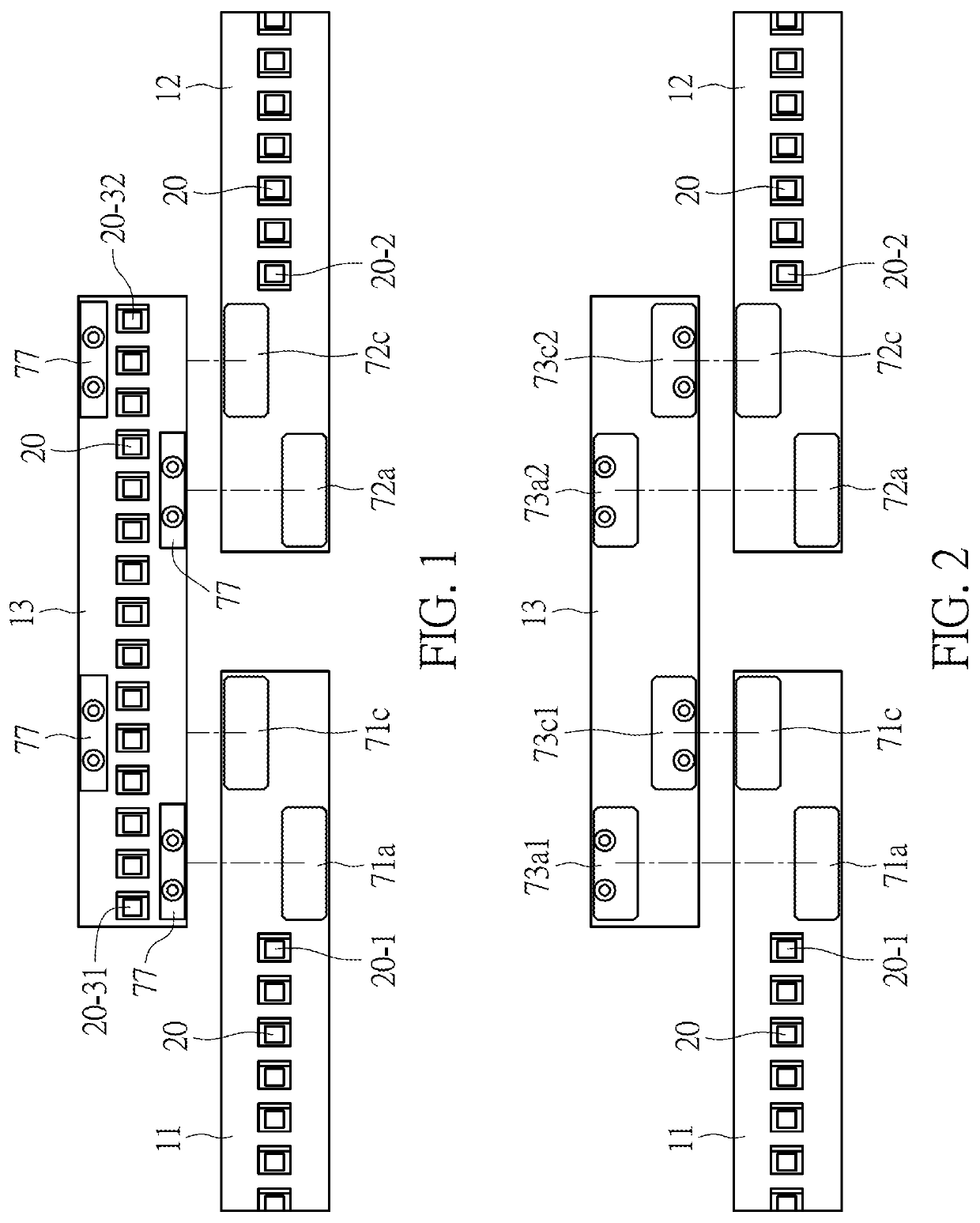
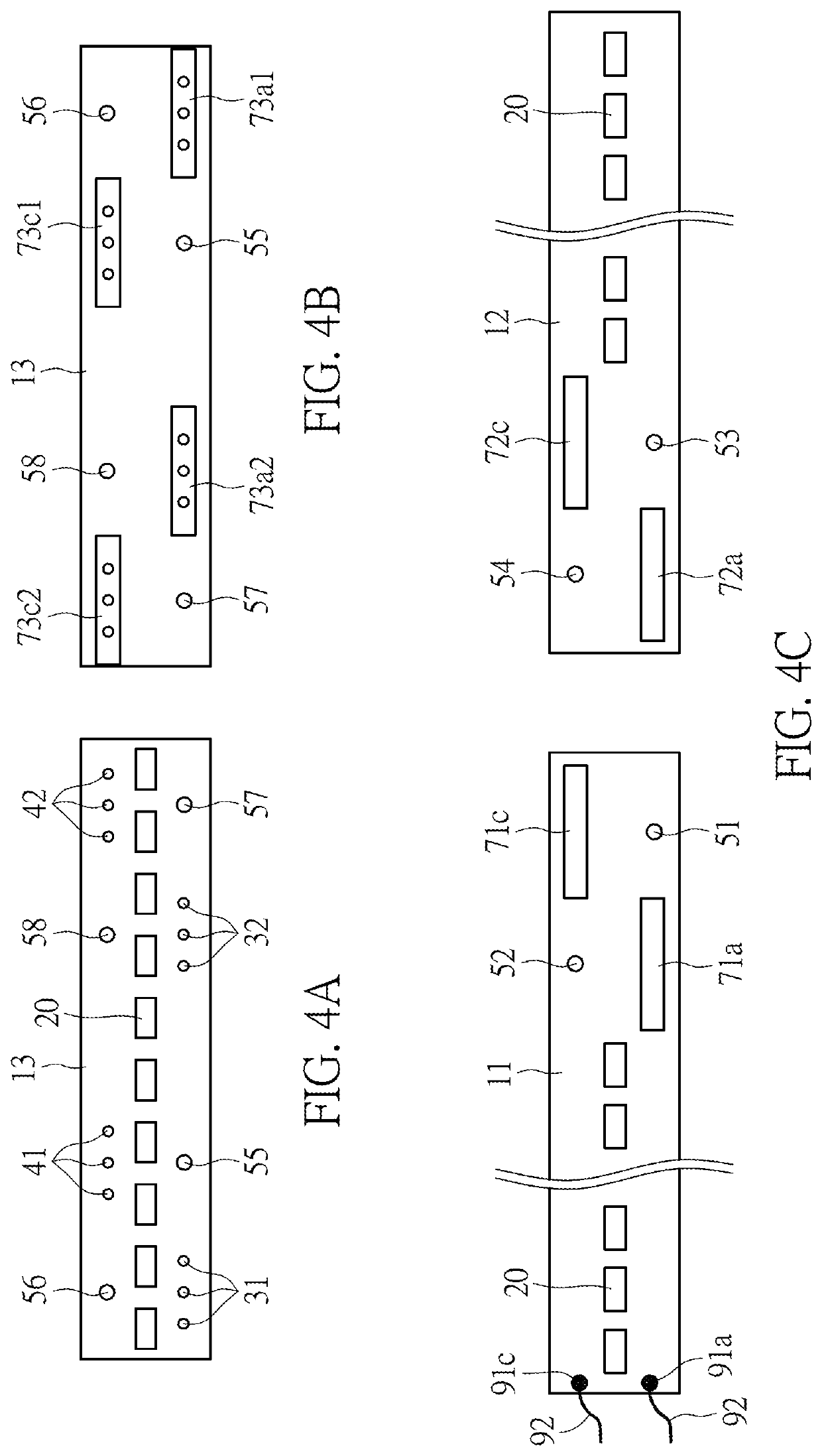
[0070]Specifically, the third positive polarity via holes 31 and the third negative polarity via holes 41 in FIG. 6A are distributed at the same side of the row of the LEDs 20, for example, below the row, as shown in FIG. 6A. Likewise, the fourth positive polarity via holes 32 and the fourth negative polarity via holes 42 are also distributed below the row of the LEDs 20. FIG. 6B shows a back surface that is presented after the connecting board 13 in FIG. 6A is turned over from left to right. Bonding zones and positioning holes marked from FIG. 6A to FIG. 6E are identical with those in the

fourth embodiment

[0071]FIG. 7A to FIG. 7E are schematic diagrams of different statuses in the present invention, where FIG. 7B shows a back surface of the connecting board 13 that is presented after the connecting board 13 in FIG. 7A is turned over from left to right; FIG. 7C shows implementation statuses of front surfaces of the first light strip 11 and the second light strip 12; FIG. 7D is a schematic diagram of an implementation status after assembly of the first light strip 11, the second light strip 12, and the connecting board 13; and FIG. 7E is a schematic side view after assembly.

[0072]In the fourth embodiment shown in FIG. 7A to FIG. 7E, a difference between this embodiment and the first embodiment is as follows: An extended bonding sector 60 is extended from a side of the connecting board 13, and is used to provide bonding zones for positive or negative power input circuits or circuit signals, so as to connect multiple corresponding LED power lines or control lines on the LED light strips....


PUM

PropertyMeasurementUnit
sizeaaaaaaaaaa
thicknessaaaaaaaaaa
heightaaaaaaaaaa

Abstract

Disclosed are a uniformly emitting linear LED light source assembly and a method thereof. The linear LED light source assembly comprises a first light strip, at least one second light strip and at least one connecting board which are all provided with a plurality of LEDs closely arranged at equal intervals, wherein the equal interval is less than 3.5 mm to realize uniform illumination. The connecting board connects the first light strip and the second light strip. The LED closest to the first light strip on the connecting board and the LED closest to the connecting board on the first light strip are formed at the same pitch as the equal interval. In addition, the LED closest to the second light bar on the connecting board and the LED closest to the connecting board on the second light bar are formed at the same pitch as the equal interval.

Description

BACKGROUND OF THE INVENTION1. Field of the Invention[0001]The present invention relates to a uniformly emitting linear light emitting diode (LED) light source assembly and a method thereof, and in particular, to a uniformly emitting linear LED light source assembly which can realize uniform illumination and can be lengthened according to usage requirements, and a method thereof.2. Description of Related Art[0002]In the LED-related lighting technology, because LEDs are energy efficient and can emit light of different colors, they have been widely applied to various fields which require illumination. Accordingly, the geometric structure of an LED light source or an LED lamp is evolved from an original point light source, to a linear light source, a surface light source or even a stereo light source according to requirements in design and usage. Thus, the LED light source is applied to almost everywhere, such as from household appliances to 3C products, display, illumination, automotiv...

Claims


Application Information

Patent Timeline
Patent Type & Authority Patents(United States)
IPC IPC(8): H05K1/00H05K1/11F21V19/00H05K1/02H05K1/09H01L33/62H01L23/538H01L25/075H05K7/00H05K1/18H05K1/14F21Y103/10F21Y115/10
CPCH01L33/62H01L25/0753H05K1/144H05K1/09F21V19/001H01L23/5387H05K1/115H05K1/028H05K2201/10106H05K2201/041F21Y2115/10F21Y2103/10F21S4/20F21V19/0025F21V21/002F21V23/06F21K9/00F21S4/24F21Y2103/33H05B33/02H05K1/148
Inventor CHEN, YEN-CHENGCHIU, TSE-WEIJAO, CHENG-TAI
Owner EXCELLENCE OPTO INC
Why Eureka
Try Eureka