Semiconductor base having a composition graded buffer layer stack

a technology of semiconductor base and buffer layer stack, which is applied in the direction of semiconductor devices, electrical appliances, transistors, etc., can solve the problems of nitride semiconductor layer crack formation or reduction in crystal quality, and the constant of these substrates is greatly different, so as to reduce the cost, shorten the growth time, and suppress the effect of crystallinity deterioration and crack elongation

Active Publication Date: 2020-03-10
SANKEN ELECTRIC CO LTD +1
View PDF26 Cites 3 Cited by
  • Summary
  • Abstract
  • Description
  • Claims
  • Application Information

AI Technical Summary

Benefits of technology

[0027]As described above, the semiconductor base according to the present invention makes it possible to suppress crystallinity deterioration and crack elongation even when the composition graded layers having degrees of the lattice constant changed larger than 0. 7% / nm are provided between the layers in the multilayer buffer layer. This makes it possible to shorten the growth time, and thus the cost can be reduced. Moreover, the semiconductor device according to the present invention can be a semiconductor device having less crystallinity deterioration and less crack elongation in the channel layer. This makes it possible to improve the yield and properties of the semiconductor device.

Problems solved by technology

However, lattice constants of these substrates are greatly different from that of the nitride semiconductor layer, and thermal expansion coefficients are also different therebetween.
As a result, the nitride semiconductor layer tends to suffer from crack formation or a reduction in crystal quality.

Method used


Image

  • Semiconductor base having a composition graded buffer layer stack
  • Semiconductor base having a composition graded buffer layer stack
  • Semiconductor base having a composition graded buffer layer stack

Examples


example 1

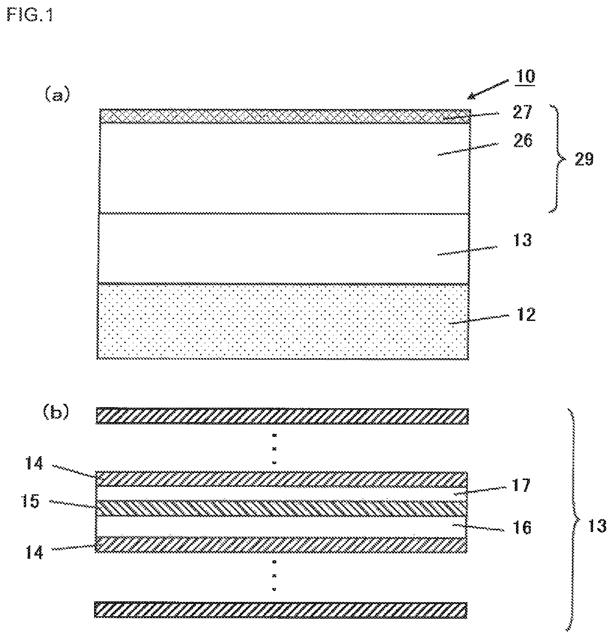
[0083]Three semiconductor bases 10 as shown in FIG. 1 were fabricated. Note that the substrate 12 was a single-crystal silicon substrate, the channel layer 26 was made of GaN, and the barrier layer 27 was made of AlGaN. Moreover, in the buffer layer 13, the first layer 14 was an AlN layer, and the second layer 15 was a GaN layer. The first composition graded layer 16 and the second composition graded layer 17 each had a composition shown by AlxGa1−xN (0≤x≤1). The distribution of an Al content rate x in the buffer layer 13 was as shown in FIG. 4. In FIG. 4, d1 represents the thickness of the first composition graded layer 16, and d2 represents the thickness of the second composition graded layer 17, satisfying a relation of d1>d2.

[0084]The degree of the lattice constant changed in the first composition graded layer 16 was 0.88% / nm, and the thickness was 2.8 nm. The degree of the lattice constant changed in the second composition graded layer 17 was larger than that in the first compo...

example 2

[0087]Three semiconductor bases were fabricated as in Example 1. Nevertheless, the degree of the lattice constant changed in the first composition graded layer 16 was 1.76% / nm, and the thickness was 1.4 nm. The degree of the lattice constant changed in the second composition graded layer 17 was larger than that in the first composition graded layer 16, the thickness of: the second composition graded layer 17 was 0.25 rim or more to less than 1.4 nm, and the degrees of the lattice constant changed were both 1.4% / nm or larger.

[0088]Using the semiconductor bases fabricated in Example 2, the crystallinity and crack length were measured as in Experimental Example 1. Table 2 shows the results.

[0089]Additionally, the above-described measurement results of Experimental Examples 1 to 3 were also shown again in Table 2 for comparison.

[0090]

TABLE 2Crystallinity:Epitaxial layerhalf-valuestructurewidth (arcsec)CrackDegree of latticeby X-raylengthconstant changeddiffraction(mm)Example 1with compo...


PUM

PropertyMeasurementUnit
thicknessaaaaaaaaaa
thicknessaaaaaaaaaa
thicknessaaaaaaaaaa

Abstract

Semiconductor base including: silicon-based substrate; buffer layer including first and second layers alternately on silicon-based substrate, first layer made of nitride-based compound semiconductor containing first material, second layer made of nitride-based compound semiconductor containing second material having larger lattice constant than first material; channel layer on buffer layer and made of nitride-based compound semiconductor containing second material, buffer layer has: first composition graded layer between at least one of first layers and second layer immediately thereabove, made of nitride-based compound semiconductor whose composition ratio of second material is increased gradually upward, whose composition ratio of first material is decreased gradually upward; second composition graded layer between at least one of second layers and first layer immediately thereabove, made of nitride-based compound semiconductor whose first material is increased gradually upward, whose composition ratio of second material is decreased gradually upward, first composition graded layer is thicker than second composition graded layer.

Description

TECHNICAL FIELD[0001]The present invention relates to a semiconductor base and a semiconductor device.BACKGROUND ART[0002]Generally, a nitride semiconductor layer is formed on an inexpensive silicon substrate or sapphire substrate. However, lattice constants of these substrates are greatly different from that of the nitride semiconductor layer, and thermal expansion coefficients are also different therebetween. Thus, considerable strain energy is produced in the nitride semiconductor layer formed on the substrate by epitaxial growth. As a result, the nitride semiconductor layer tends to suffer from crack formation or a reduction in crystal quality.[0003]To solve the problem, as a conventional practice, a buffer layer in which nitride semiconductor layers with different compositions are stacked is arranged between a substrate and a functional layer made of a nitride semiconductor.[0004]Moreover, as disclosed in Patent Documents 1 to 3 and so forth, a GaN-on-Si-based semiconductor is ...

Claims


Application Information

Patent Timeline
Patent Type & Authority Patents(United States)
IPC IPC(8): H01L29/10H01L29/205H01L21/02H01L29/20H01L29/778H01L29/66
CPCH01L21/0254H01L21/0251H01L21/02381H01L29/1075H01L21/02458H01L29/7786H01L21/02507H01L29/205H01L29/66462H01L29/2003H01L29/7787
Inventor SHIKAUCHI, HIROSHISATO, KENSHINOMIYA, MASARUTSUCHIYA, KEITAROHAGIMOTO, KAZUNORI
Owner SANKEN ELECTRIC CO LTD
Why Eureka
Try Eureka