Imaging device

a technology of a device and an image, which is applied in the direction of radio frequency controlled devices, transistors, television systems, etc., can solve problems such as and achieve the effect of deterioration of obtained images caused by nois

Active Publication Date: 2020-04-07
PANASONIC INTELLECTUAL PROPERTY MANAGEMENT CO LTD
View PDF22 Cites 2 Cited by
  • Summary
  • Abstract
  • Description
  • Claims
  • Application Information

AI Technical Summary

Benefits of technology

[0004]If charges that are different from signal charges expressing an image flow into diffusion regions temporarily storing signals charges, this can lead to noise. Noise causes deterioration of the obtained image. It is advantageous to be able to suppress unintended movement of charges. Hereinafter, such unintended movement of charges may be referred to as a leak current.

Problems solved by technology

If charges that are different from signal charges expressing an image flow into diffusion regions temporarily storing signals charges, this can lead to noise.
Noise causes deterioration of the obtained image.

Method used


Image

  • Imaging device
  • Imaging device
  • Imaging device

Examples


first embodiment

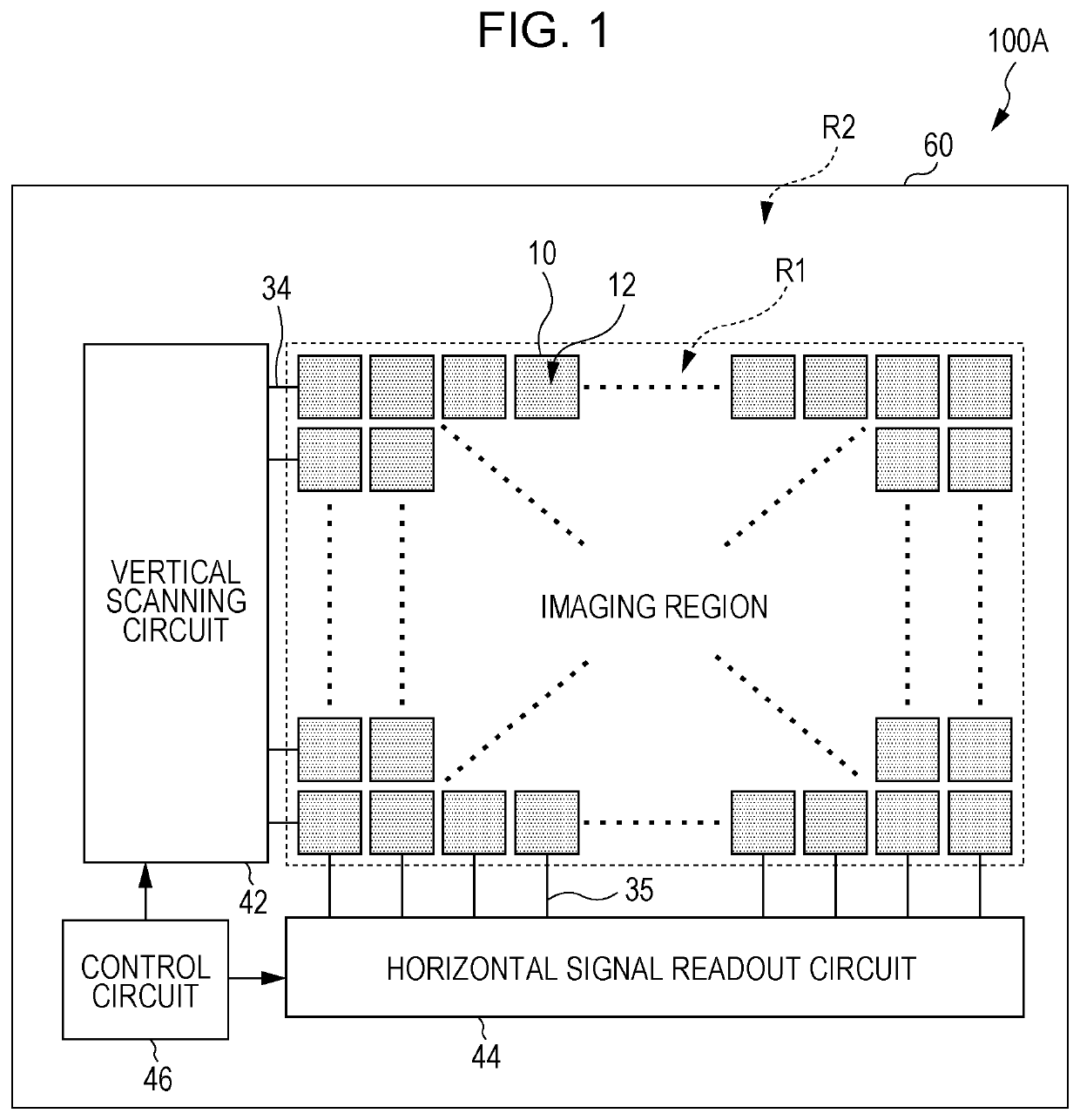
[0157]FIG. 1 illustrates an exemplary configuration of an imaging device according to a first embodiment of the present disclosure. The imaging device 100A illustrated in FIG. 1 has multiple pixels 10 formed on a semiconductor substrate 60, and peripheral circuits.

[0158]The pixels 10 each include a photoelectric converter 12. The photoelectric converter 12 receives incident light, and generates positive and negative charges, typically a hole-electron pair. The photoelectric converter 12 may be a photoelectric conversion structure including a photoelectric conversion layer disposed above the semiconductor substrate 60, and may be a photodiode formed on the semiconductor substrate 60. Although the photoelectric converters 12 of the pixels 10 are illustrated in FIG. 1 as being spatially separated from each other, but this is only for convenience in describing, and the photoelectric converters 12 of the multiple pixel 10 may be continuously laid out on the semiconductor substrate 60 wit...

first modification

[0206]FIG. 3B schematically illustrates an exemplary configuration of the imaging device according to a first modification of the first embodiment. The primary difference between the pixel As illustrated in FIG. 3B and the pixel 10A described with reference to FIG. 3A is that in the pixel As, a p-type semiconductor layer 63ps is provided in the semiconductor substrate 60A instead of the p-type semiconductor layer 63p.

[0207]The p-type semiconductor layer 63ps is formed in a region other than directly below the impurity region 69n on the n-type semiconductor layer 62n, as schematically illustrated in FIG. 3B. In other words, the p-type semiconductor layer 63ps has an opening at the portion directly below the impurity region 69n. The impurity region 69pa that is part of the p-type impurity region 66p is located inside this opening, as illustrated in FIG. 3B.

[0208]As described above, the concentration of impurity of the p-type impurity region 66p is lower in comparison with the p-type ...

second modification

[0209]FIG. 4 schematically illustrates an exemplary configuration of the imaging device according to the second modification of the first embodiment. The imaging device 100B illustrated in FIG. 4 further has a voltage supply circuit 48 disposed in the peripheral region R2 as compared with the imaging device 100A illustrated in FIG. 1.

[0210]The voltage supply circuit 48 supplies a predetermined voltage to the pixels 10 via a voltage line 38, based on drive signals from the control circuit 46, as schematically illustrated in FIG. 4. The voltage supply circuit 48 is not restricted to a particular power source circuit, and may be a circuit that converts voltage supplied from a power source such as a battery to a predetermined voltage, or may be a circuit that generates a predetermined voltage. The voltage supply circuit 48 may be part of the above-described vertical scanning circuit 42.

[0211]FIG. 5 schematically illustrates the device structure of a pixel that the imaging device 100b il...


PUM

PropertyMeasurementUnit
voltageaaaaaaaaaa
voltageaaaaaaaaaa
voltage VDDaaaaaaaaaa

Abstract

An imaging device according to the present disclosure includes: a photoelectric converter that generates signal charge; a semiconductor substrate including a first semiconductor layer containing an impurity of a first conductivity type and an impurity of a second conductivity type; and a first transistor including a first impurity region of the second conductivity type in the first semiconductor layer. The first semiconductor layer includes: a charge accumulation region of the second conductivity type, for accumulating the signal charge; and a blocking structure between the charge accumulation region and the first transistor. The blocking structure includes a second impurity region of the first conductivity type, a third impurity region of the second conductivity type, and a fourth impurity region of the first conductivity type, which are arranged in that order in a direction from the first impurity region toward the charge accumulation region, at the surface of the first semiconductor layer.

Description

BACKGROUND1. Technical Field[0001]The present disclosure relates to an imaging device.2. Description of the Related Art[0002]Charge-coupled device (CCD) image sensors and complementary metal-oxide semiconductor (CMOS) image sensors are in widespread use in digital cameras and the like. These image sensors have photodiodes formed on a semiconductor substrate, which is a well-known fact.[0003]A structure is being proposed where a photoelectric conversion layer is disposed above the semiconductor substrate instead of the photodiodes, as disclosed in International Publication Nos. 2014 / 002330 and 2012 / 147302, for example. Imaging device that have this sort of structure may be referred to as stacked imaging devices. In a stacked imaging device, charges generated by photoelectric conversion are temporarily accumulated in diffusion regions and the like formed in the semiconductor substrate, as signal charges. Signals corresponding to the amount of charges accumulated are read out via a CCD...

Claims


Application Information

Patent Timeline
Patent Type & Authority Patents(United States)
IPC IPC(8): H01L27/146H01L27/30H04N5/369H04N5/359
CPCH01L27/307H01L27/14603H04N5/379H01L27/14609H04N5/359H01L27/1463H01L27/14612H01L27/14665H04N25/79H04N25/62H10K39/32
Inventor HIRASE, JUNJITAKAMI, YOSHINORISATO, YOSHIHIRO
Owner PANASONIC INTELLECTUAL PROPERTY MANAGEMENT CO LTD
Why Eureka
Try Eureka