Imaging device

a technology of a device and an image, which is applied in the direction of radio frequency controlled devices, transistors, television systems, etc., can solve problems such as and achieve the effect of deterioration of obtained images caused by nois

Active Publication Date: 2021-01-12
PANASONIC INTELLECTUAL PROPERTY MANAGEMENT CO LTD
View PDF23 Cites 1 Cited by
  • Summary
  • Abstract
  • Description
  • Claims
  • Application Information

AI Technical Summary

Benefits of technology

[0004]If charges that are different from signal charges expressing an image flow into diffusion regions temporarily storing signals charges, this can lead to noise. Noise causes deterioration of the obtained image. It is advantageous to be able to suppress unintended movement of charges. Hereinafter, such unintended movement of charges may be referred to as a leak current.

Problems solved by technology

If charges that are different from signal charges expressing an image flow into diffusion regions temporarily storing signals charges, this can lead to noise.
Noise causes deterioration of the obtained image.

Method used


Image

  • Imaging device
  • Imaging device
  • Imaging device

Examples


first embodiment

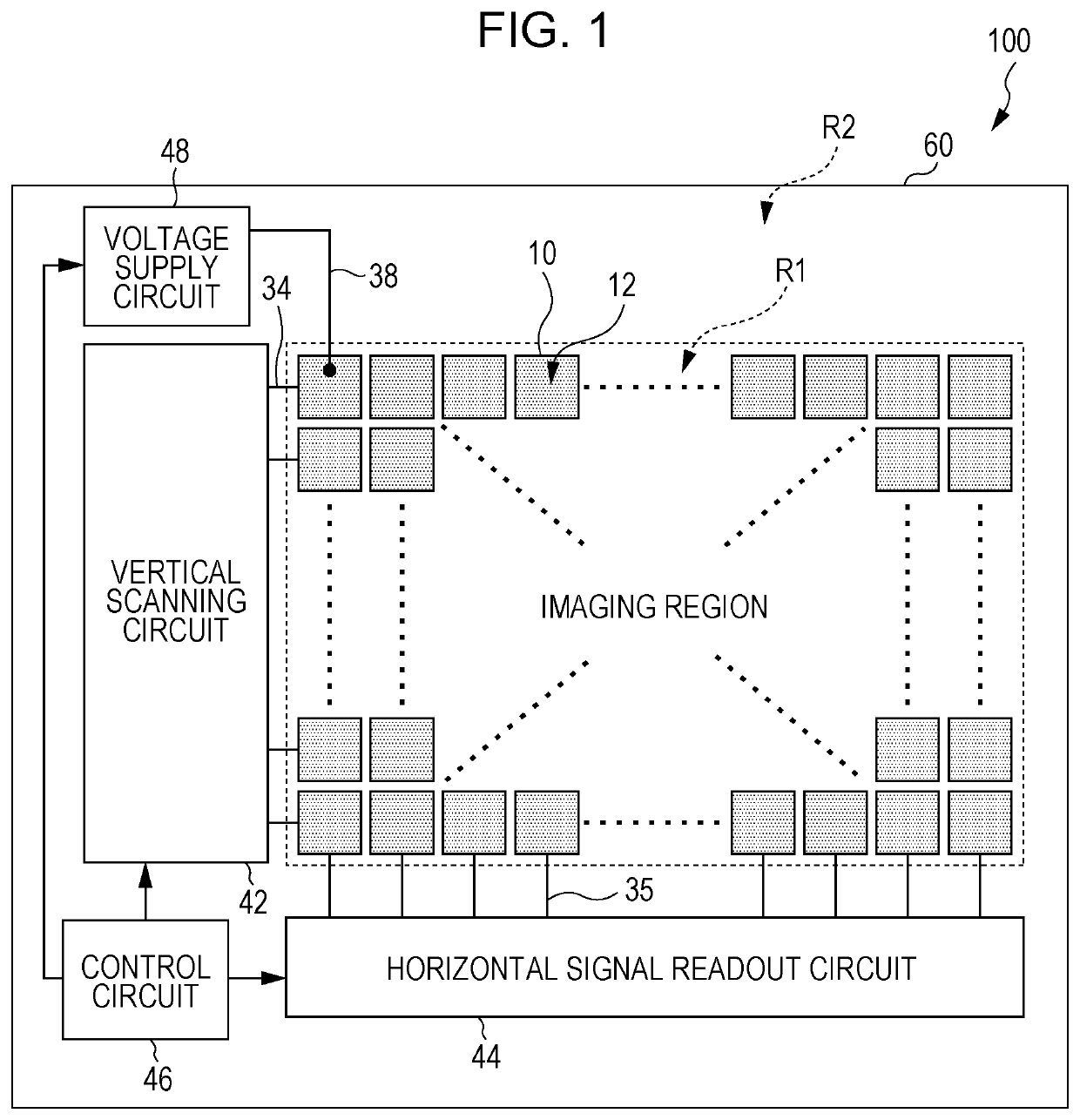
[0156]FIG. 1 illustrates an exemplary configuration of an imaging device according to a first embodiment of the present disclosure. The imaging device 100 illustrated in FIG. 1 has multiple pixels 10 formed on a semiconductor substrate 60, and peripheral circuits.

[0157]The pixels 10 each include a photoelectric converter 12. The photoelectric converter 12 receives incident light, and generates positive and negative charges, typically a hole-electron pair. The photoelectric converter 12 may be a photoelectric conversion structure including a photoelectric conversion layer disposed above the semiconductor substrate 60, and may be a photodiode formed on the semiconductor substrate 60. Although the photoelectric converters 12 of the pixel 10 are illustrated in FIG. 1 spatially separated from each other, but this is only for convenience in describing, and the photoelectric converters 12 of the multiple pixels 10 may be continuously laid out on the semiconductor substrate 60 without spaci...

first modification

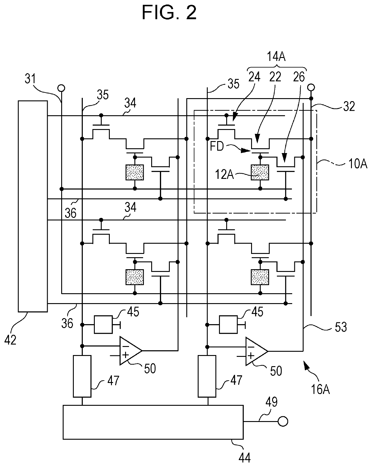
[0212]FIGS. 6 and 7 illustrate an imaging device according to a first modification of the first embodiment of the present disclosure. FIG. 6 illustrates an example of the layout of elements in a pixel 10B that the imaging device according to the first embodiment has, and FIG. 7 illustrates an exemplary circuit configuration of the pixel 10B illustrated in FIG. 6.

[0213]The pixel 10B illustrated in FIGS. 6 and 7 has a photodiode 12B as the photoelectric converter 12 instead of the photoelectric conversion structure 12A, as compared with the pixel 10A described with reference to FIGS. 2 through 4. In this example, the accumulation control line 31 illustrated in FIG. 2 is omitted. The point of one of the drain and source of the reset transistor 26 being connected to the charge accumulation node FD is the same as the configuration illustrated in FIG. 2. Note, however, that the power source wiring 32 is connected to the other of the drain and source of the reset transistor 26 here.

[0214]T...

second modification

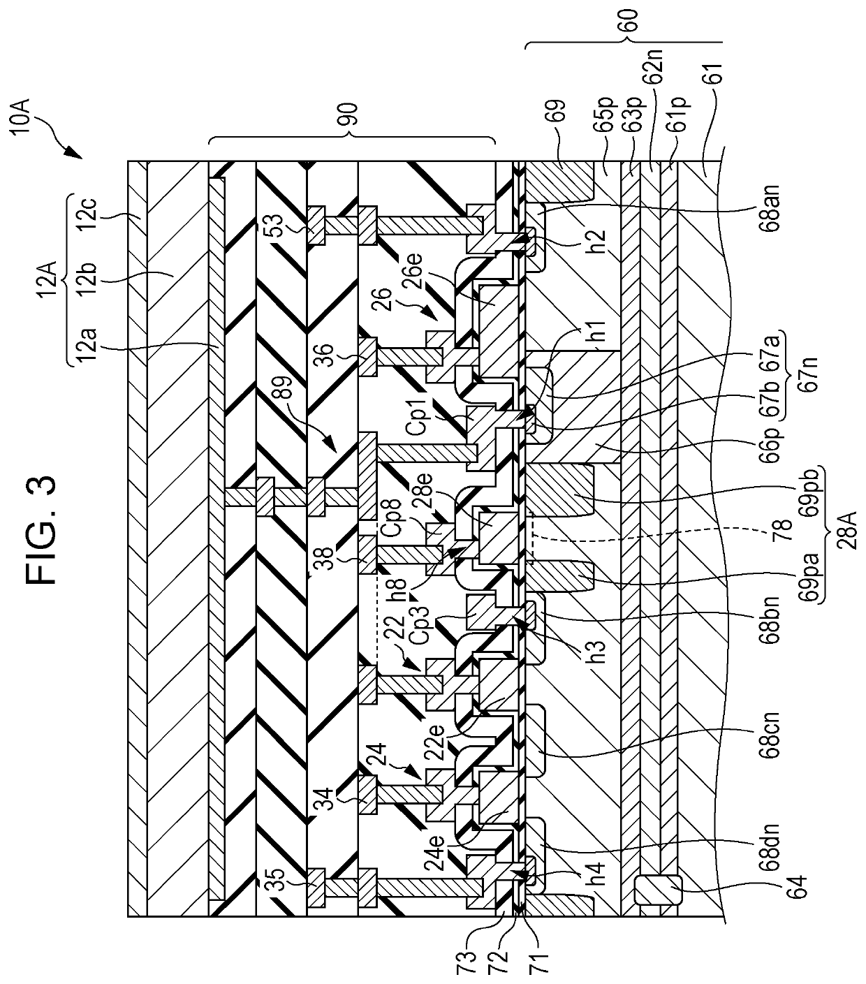
[0217]FIG. 8 illustrates a second modification of the imaging device according to the first embodiment of the present disclosure. FIG. 8 illustrates an example of layout of elements in a pixel 10C that the imaging device according to the second modification has.

[0218]The primary point of difference between the pixel 10C illustrated in FIG. 8 and the pixel 10A illustrated in FIG. 4 is that the pixel 10C has the reset signal line 36 connected to the control electrode 28e instead of the voltage line 38. That is to say, in this example, the control electrode 28e is equipotential with the gate electrode 26e of the reset transistor 26.

[0219]In this example, the vertical scanning circuit 42 also has the functions of the above-described voltage supply circuit 48. Connecting the reset signal line 36 to the control electrode 28e enables the voltage line 38 and the voltage supply circuit 48 to be omitted, as exemplified in FIG. 8. Accordingly, effects of suppressing leak current can be obtaine...


PUM

PropertyMeasurementUnit
voltageaaaaaaaaaa
voltage VDDaaaaaaaaaa
voltageaaaaaaaaaa

Abstract

An imaging device according to the present disclosure includes: a photoelectric converter generating signal charge; a semiconductor substrate including a first semiconductor layer on a surface; a charge accumulation region of a first conductivity type in the first semiconductor layer; a first transistor including, as a source or a drain, a first impurity region of the first conductivity type in the first semiconductor layer; and a blocking structure between the charge accumulation region and the first transistor. The blocking structure includes a second impurity region of a second conductivity type in the first semiconductor layer, between the charge accumulation region and the first impurity region, and a first electrode above the first semiconductor layer, overlapping at least part of the second impurity region in plan view, the first electrode being configured to be applied with a constant voltage in a period when the charge accumulation region accumulates the signal charge.

Description

BACKGROUND1. Technical Field[0001]The present disclosure relates to an imaging device.2. Description of the Related Art[0002]Charge-coupled device (CCD) image sensors and complementary metal-oxide semiconductor (CMOS) image sensors are in widespread use in digital cameras and the like. These image sensors have photodiodes formed on a semiconductor substrate, which is a well-known fact.[0003]A structure is being proposed where a photoelectric conversion layer is disposed above the semiconductor substrate instead of the photodiodes, as disclosed in International Publication Nos. 2014 / 002330 and 2012 / 147302, for example. Imaging device that has this sort of structure may be referred to as stacked imaging devices. In a stacked imaging device, charges generated by photoelectric conversion are temporarily accumulated in diffusion regions and the like formed in the semiconductor substrate, as signal charges. Signals corresponding to the amount of charges accumulated are read out via a CCD ...

Claims


Application Information

Patent Timeline
Patent Type & Authority Patents(United States)
IPC IPC(8): H01L27/146H04N5/359H01L27/30H04N5/369
CPCH01L27/14603H01L27/1461H01L27/14609H01L27/14612H01L27/14614H01L27/14616H01L27/14636H01L27/14638H01L27/307H04N5/359H04N5/379H01L27/146H01L27/14601H01L27/14643H01L27/14665H04N25/65H10K39/32H01L27/1463H04N25/62H04N25/79
Inventor SATO, YOSHIHIROHIRASE, JUNJI
Owner PANASONIC INTELLECTUAL PROPERTY MANAGEMENT CO LTD
Why Eureka
Try Eureka