Semiconductor method having annealing of epitaxially grown layers to form semiconductor structure with low dislocation density

a semiconductor structure and epitaxial growth technology, applied in the direction of crystal growth process, polycrystalline material growth, chemically reactive gas, etc., can solve the problem of high cost of uv led production in large quantities, and achieve the effect of low cost and low dislocation density

Active Publication Date: 2020-04-21
SENSOR ELECTRONICS TECH
View PDF14 Cites 0 Cited by
  • Summary
  • Abstract
  • Description
  • Claims
  • Application Information

AI Technical Summary

Benefits of technology

[0005]Aspects of the present invention are directed to improving the performance of optoelectronic devices and / or extending the operational lifetime of the devices by annealing semiconductor structures used to fabricate the devices. Annealing minimizes dislocation density and the number of cracks formed in the semiconductor structures, which leads to better performance of the optoelectronic devices and increases the operational lifetime of the devices. In one embodiment, a semiconductor structure of one the embodiments described herein that can have a low dislocation density through annealing can include a substrate, a nucleation layer of group III nitride semiconductor material formed on the substrate, a buffer layer epitaxially grown at a first temperature T1 on the nucleation layer and annealed at a second temperature T2 that is greater than the first temperature T1, and at least one semiconductor layer formed on the annealed buffer layer that is part of a semiconductor heterostructure (e.g., n-type semiconductor layer, light generating layer and p-type semiconductor layer) used to fabricate an optoelectronic device.
[0018]In one embodiment, multiple substrates (e.g., wafers) can be used to epitaxially grow multiple buffer layers. For example, a large commercial MOCVD chamber can be used to process many wafers at once in order to attain a plurality of buffer layers that can be used to reduce the dislocation density and improve the quality of semiconductor layers formed on these buffer layers. The wafers can then be removed and stacked to ensure that each buffer layer cannot be easily desorbed during annealing. Such a stacked configuration can be placed in a chamber (e.g., an annealing chamber) and annealed to form a template structure (i.e., a buffer layer over a substrate) that can be used for the subsequent growth of the semiconductor layers in the heterostructure of an optoelectronic device.

Problems solved by technology

While substrate patterning is a common route to achieving higher quality epitaxial layers, this approach is expensive for production of UV LEDs in large quantities, and does not necessary translate into improvements in performance and reliability.

Method used


Image

  • Semiconductor method having annealing of epitaxially grown layers to form semiconductor structure with low dislocation density
  • Semiconductor method having annealing of epitaxially grown layers to form semiconductor structure with low dislocation density
  • Semiconductor method having annealing of epitaxially grown layers to form semiconductor structure with low dislocation density

Examples


Embodiment Construction

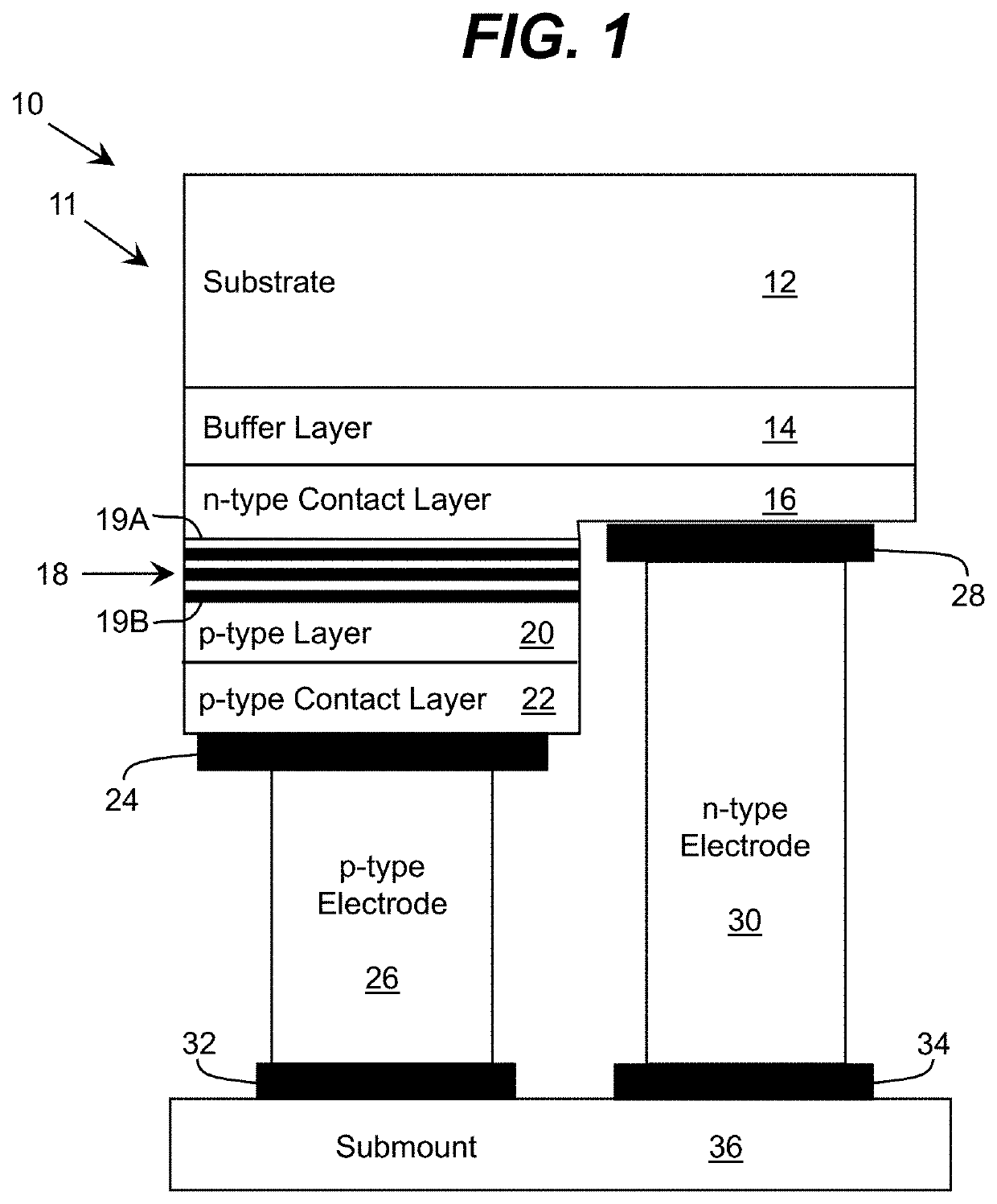
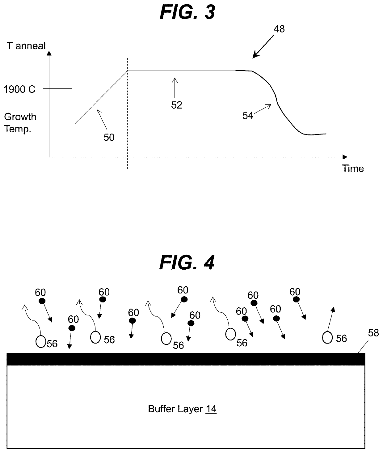
[0043]As indicated above, aspects of the present invention are directed to improving the performance of optoelectronic devices and / or extending the operational lifetime of the devices by annealing semiconductor structures used to fabricate the devices. The annealing minimizes dislocation density and the number of cracks formed in the semiconductor structures, which leads to better optoelectronic device performance and increases the operational lifetime of the device.

[0044]A layer of any of the semiconductor structures described herein can be considered to be transparent to radiation of a particular wavelength when the layer allows an amount of the radiation radiated at a normal incidence to an interface of the layer to pass there through. For example, a layer can be configured to be transparent to a range of radiation wavelengths corresponding to a peak emission wavelength for light, such as ultraviolet light or deep ultraviolet light, emitted by a light generating structure (e.g., ...


PUM

PropertyMeasurementUnit
radiation wavelengthsaaaaaaaaaa
transparentaaaaaaaaaa

Abstract

Semiconductor structures formed with annealing for use in the fabrication of optoelectronic devices. The semiconductor structures can include a substrate, a nucleation layer and a buffer layer. The nucleation layer and the buffer layer can be epitaxially grown and then annealed. The temperature of the annealing of the nucleation layer and the buffer layer is greater than the temperature of the epitaxial growth of the layers. The annealing reduces the dislocation density in any subsequent layers that are added to the semiconductor structures. A desorption minimizing layer epitaxially grown on the buffer layer can be used to minimize desorption during the annealing of the layer which also aids in curtailing dislocation density and cracks in the semiconductor structures.

Description

REFERENCE TO RELATED APPLICATIONS[0001]The present patent application claims the benefit of U.S. Provisional Application No. 62 / 528,001, filed on 30 Jun. 2017, which is hereby incorporated by reference in its entirety to provide continuity of disclosure.TECHNICAL FIELD[0002]The disclosure relates generally to semiconductor-based devices, and more particularly, to optoelectronic devices formed with semiconductor heterostructures having structures annealed to reduce dislocation density in the structures and in other semiconductor layers formed on the structures.BACKGROUND ART[0003]Semiconductor-based optoelectronic devices, such as semiconductor emitting and sensing devices, can include light emitting diodes (LEDs) composed of group III-V semiconductors. Ultraviolet (UV) LEDs based on group III nitride semiconductor layers are a subset of LEDs composed of group III-V semiconductors. The performance and reliability of UV LED devices based on group III nitride semiconductor layers are d...

Claims


Application Information

Patent Timeline
Patent Type & Authority Patents(United States)
IPC IPC(8): H01L21/02H01L33/00H01L31/18C30B29/68C23C16/30C23C16/56C30B25/18C23C16/34C23C16/02C30B29/40H01L33/12H01L33/32
CPCC30B29/406C30B29/68H01L21/02505C23C16/34H01L31/1848H01L33/007H01L31/1852C23C16/303C23C16/0272H01L31/1856H01L33/0075C23C16/56C30B25/186C30B29/403C30B25/183H01L21/0254H01L21/02458H01L31/1864H01L33/32H01L33/12
Inventor JAIN, RAKESHSHATALOV, MAXIM S.
Owner SENSOR ELECTRONICS TECH
Why Eureka
Try Eureka