Distributive photonic monobit analog-to-digital converter

a technology of photonic monobits and converters, applied in the field of analog-to-digital converters (adcs), can solve problems such as difficulties in achieving

Active Publication Date: 2020-06-30
RAYTHEON CO
View PDF46 Cites 6 Cited by
  • Summary
  • Abstract
  • Description
  • Claims
  • Application Information

AI Technical Summary

Problems solved by technology

High bandwidth and high spur-free dynamic range analog-to-digital conversion is a common desire across multiple domains but is difficult to achieve.

Method used


Image

  • Distributive photonic monobit analog-to-digital converter
  • Distributive photonic monobit analog-to-digital converter
  • Distributive photonic monobit analog-to-digital converter

Examples


Embodiment Construction

[0011]The following description and the drawings sufficiently illustrate aspects to enable those skilled in the art to practice them. Other aspects may incorporate structural, logical, electrical, process, and other changes. Portions and features of some aspects may be included in, or substituted for, those of other aspects. Aspects set forth in the claims encompass all available equivalents of those claims.

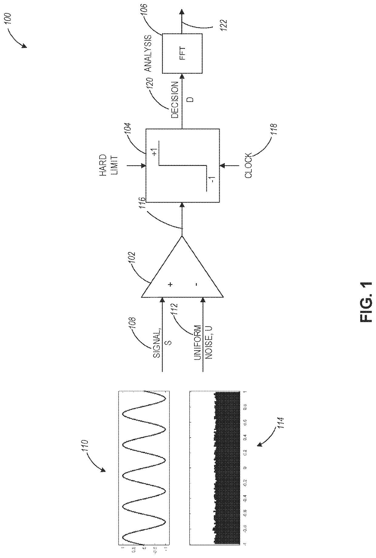
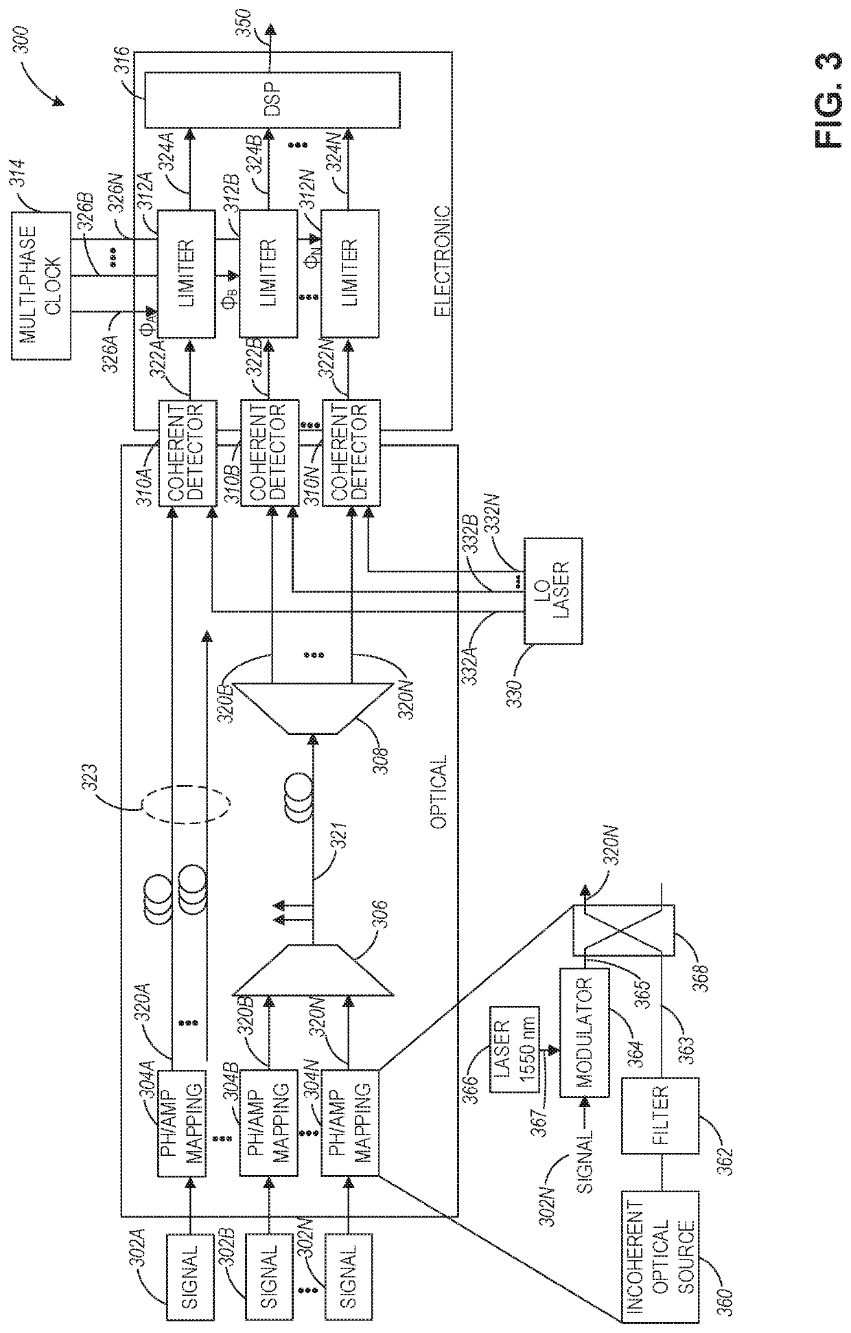
[0012]Techniques disclosed herein can be used to realize a photonic ADC with high spur-free dynamic range (SFDR) based on a monobit concept, such as dithering an input signal with uniform noise. Furthermore, techniques disclosed herein can use distributive analog-to-digital conversion where multiple remote RF signals are sampled, and after photonic monobit conversion, are multiplexed and transmitted via an optical medium. In this regard, an optical waveform can be transmitted over a large distance to a digital signal processing location. At the digital signal processing location,...


PUM

PropertyMeasurementUnit
wavelengthaaaaaaaaaa
frequencyaaaaaaaaaa
frequencyaaaaaaaaaa

Abstract

A distributive photonic monobit analog-to-digital converter includes a plurality of signal processing chains configured to receive a corresponding plurality of analog input electrical signals. Each processing chain includes an incoherent optical source configured to generate an optical noise signal, an optical modulator configured to modulate an analog input electrical signal of the plurality of analog input electrical signals onto an input optical signal to generate an optical modulated signal, a coupler configured to couple the optical modulated signal with the optical noise signal to generate a coupled signal, a photodetector configured to generate a phase difference between the optical modulated signal and the optical noise signal using the coupled signal, and a limiter configured to output a decision signal based on the phase difference and using a clock signal. A multi-phase clock generator is configured to generate the clock signal for each of the plurality of signal processing chains.

Description

TECHNICAL FIELD OF THE DISCLOSURE[0001]The present disclosure relates to analog-to-digital converters (ADCs). More specifically, the present disclosure relates to distributive photonic monobit ADCs, such as photonic monobit ADCs using coherent or balanced detection.BACKGROUND OF THE DISCLOSURE[0002]As communication systems evolve over time, digital data rates tend to increase. As a result, there is an ongoing effort to increase the speed and accuracy of analog-to-digital conversion to support the increase in communication rates.[0003]High bandwidth and high spur-free dynamic range analog-to-digital conversion is a common desire across multiple domains but is difficult to achieve. With the advent of photonics, the analog-to-digital conversion can be improved beyond the electronic conversion by harvesting the photonics bandwidth and balancing the functional partition between electronics and photonics.BRIEF DESCRIPTION OF THE DRAWINGS[0004]FIG. 1 illustrates a conceptual block diagram ...

Claims


Application Information

Patent Timeline
Patent Type & Authority Patents(United States)
IPC IPC(8): H03M1/00G02F7/00H03M3/00H03M1/36
CPCG02F7/00H03M1/001H03M1/361H03M3/468H03M1/04
Inventor SHAMEE, BISHARAWILKINSON, STEVEN R.
Owner RAYTHEON CO
Why Eureka
Try Eureka