Silicon-photonics-based optical switch with low polarization sensitivity

a technology of optical switch and polarization sensitivity, applied in the field of optical switch, can solve the problems of high optical loss of these switches, difficult scaling of datacenter networks to support such expansion with current electronic switches, and high energy consumption, cost and latency become serious issues, and achieve low polarization dependence, high port count, and high optical switching efficiency.

Active Publication Date: 2020-07-14
RGT UNIV OF CALIFORNIA
View PDF22 Cites 6 Cited by
  • Summary
  • Abstract
  • Description
  • Claims
  • Application Information

AI Technical Summary

Benefits of technology

[0013]The present invention enables rapid, low-loss optical switching in a low-cost, practical switch technology to effect an optical switching system having substantially lower polarization dependence and / or substantially higher port count than achievable in the prior art. Embodiments of the present invention include cross-bar switching elements comprising bus waveguides formed on different planes above a substrate, which eliminates the need for polarization-dependent elements and duplicate switching fabrics for polarization-diverse operation. As a result, the present invention enables switching systems that are well suited for use in telecom and datacom optical circuit switches, such as optical cross connects, wavelength-selective cross connects, reconfigurable optical add-drop multiplexers, 1×2 switches, 2×2 switches, and the like.
[0014]An illustrative embodiment of the present invention is a silicon-photonics optical cross-connect that includes an arrangement of 2×2 switching cells disposed on a substrate, where each switching cell includes a pair of fixed-position bus waveguides and a movable shunt waveguide coupled with an actuator that is operative for optically coupling and decoupling the shunt waveguide with the bus waveguides. The first bus waveguide is formed in a first plane above the substrate and includes a first input to the switching cell and a first output. The second bus waveguide is formed in a second plane above the substrate and includes a second input and a second output. Since the first and second bus waveguides lie in different planes above the substrate, they are not optically coupled when the switching cell is in its unswitched state, which avoids the polarization sensitivity associated with prior-art waveguide crossings. Furthermore, each of the bus waveguides and the shunt waveguide has a surface waveguide structure that mitigates their polarization sensitivity.

Problems solved by technology

Scaling of datacenter networks to support such expansion with current electronic switches is challenging as the link rate increases to 100 Gb / s and beyond.
The energy consumption, cost, and latency become serious issues.
Unfortunately, the optical loss of these switches is excessively high, around 16 dB for a 32×32 switch.
Such high loss exceeds the loss budget of most fiber optic links, which prevent them from being used in data center networks.
Unfortunately, silicon-photonic systems of the prior art are normally characterized by significant polarization sensitivity, which gives rise to large differences in their propagation and insertion losses for different polarization modes—referred to polarization-dependent loss (PDL).
Many applications, such as fast optical circuit switches for scalable and reconfigurable datacenter networks, among others, require very low PDL, however.
As a result, silicon-photonic based optical switching systems have found little traction in such applications and their use has been substantially limited to single-polarization systems.
It should be noted, however, while the use of thick waveguides affords reduced polarization sensitivity, it is achieved at the expense of lower integration density.
Furthermore, the systems disclosed by Nakamura et al rely up on a switch architecture comprising cascaded stages of 1×2 and 2×2 Mach-Zehnder interferometers, which gives rise to high cumulative losses for large-port-count arrangements.
Unfortunately, such systems required the use of external (off-chip) polarization splitters / combiners, which are bulky, or directional couplers as on-chip polarization splitters and combiners; however, it still requires two sets of switches and complex crossing waveguides to route the TE and TM signals.
Most importantly, all such prior-art polarization-diverse switches use many stages of cascaded 2×2 switches, which leads to high insertion loss at high port count, thus limiting their scalability to high radix switches.
A second issue of silicon photonic switch is size of the switch known as the port count or radix of the switch.
A practical, fast, low-cost, low-loss optical switching technology that has low polarization-dependent loss and scalable to high port count is, as yet, unavailable in the prior art.

Method used


Image

  • Silicon-photonics-based optical switch with low polarization sensitivity
  • Silicon-photonics-based optical switch with low polarization sensitivity
  • Silicon-photonics-based optical switch with low polarization sensitivity

Examples


Embodiment Construction

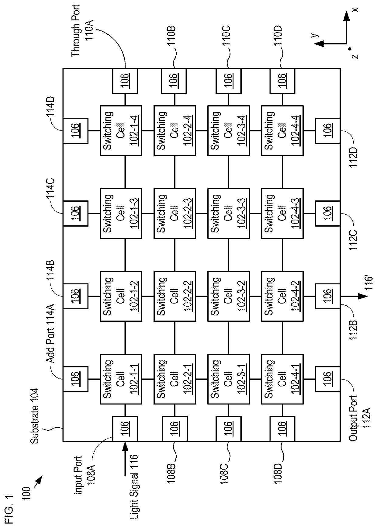
[0045]FIG. 1 depicts a schematic drawing of an optical switching system in accordance with an illustrative embodiment of the present invention. System 100 is an optical cross-connect that includes a 4×4 array of switching-cells 102-1-1 through 102-4-4, each of which is disposed on substrate 104. It should be noted that, although the depicted example comprises three rows and four columns of switching cells, any practical number of rows and / or columns of switching cells can be included in system 100 without departing from the scope of the present invention.

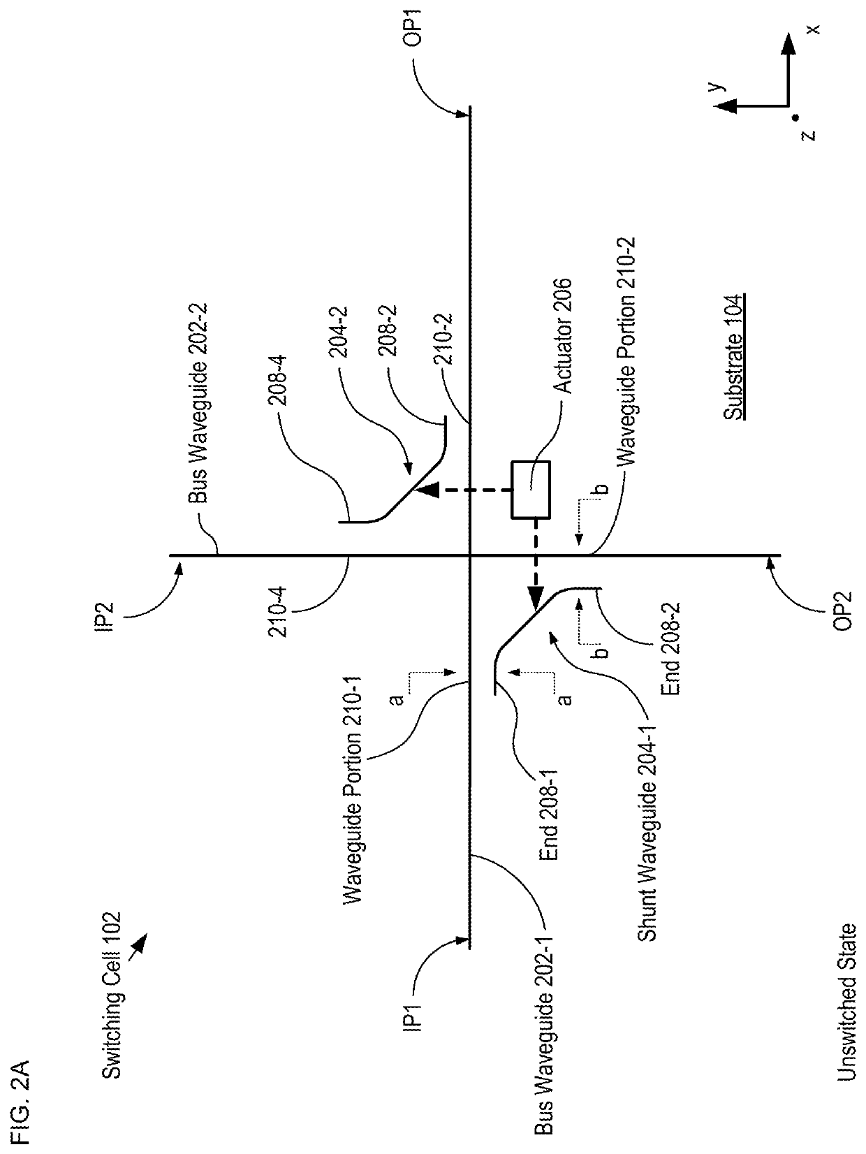
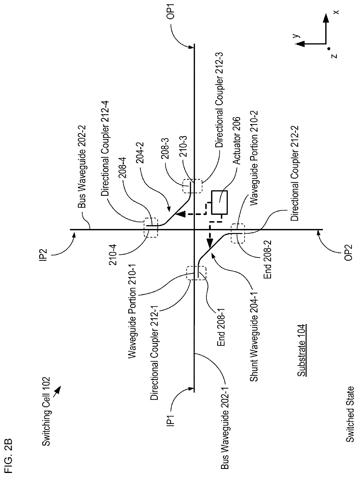
[0046]Each of switching cells 102-1-1 through 102-4-4 (referred to, collectively, as cells 102) is a 2×2 crossbar switch that includes a pair of sub-micron-width bus waveguides and a pair of movable shunt waveguides, whose positions determine the connectivity of the inputs and outputs of the switching cell.

[0047]It is an aspect of the present invention that the silicon-photonic waveguides used in the switching cells of its different...


PUM

PropertyMeasurementUnit
insertion lossaaaaaaaaaa
widthaaaaaaaaaa
widthaaaaaaaaaa

Abstract

A polarization-independent optical switching system capable of rerouting light signals is disclosed. The system includes a plurality of switching cells, each including a pair of bus waveguides that are formed in different planes above a substrate. Each bus waveguide supports low-loss propagation of both the TE- and TM-polarization modes and are optically decoupled when the switch is in an unswitched state. In its switched state, a shunt waveguide that also supports low-loss propagation of both polarization modes is moved into proximity with both bus waveguides to form a pair of adiabatic directional couplers that enable the light signal to evanescently couple between each bus waveguide and the shunt waveguide. As a result, the path of a light signal through the switching cell is reconfigured.

Description

CROSS REFERENCE TO RELATED APPLICATIONS[0001]This case claims priority of U.S. Provisional Patent Application Ser. No. 62 / 385,343, filed Sep. 9, 2016, which is incorporated herein by reference.[0002]If there are any contradictions or inconsistencies in language between this application and one or more of the cases that have been incorporated by reference that might affect the interpretation of the claims in this case, the claims in this case should be interpreted to be consistent with the language in this case.STATEMENT REGARDING FEDERALLY SPONSORED RESEARCH[0003]This invention was made with Government support under Contract Nos. HR0011-11-2-0021 and HR0011-17-1-0001 awarded by the Defense Advanced Projects Research Agency (DARPA) and Grant No. EEC0812072 awarded by the National Science Foundation (NSF). The Government has certain rights in the invention.FIELD OF THE INVENTION[0004]The present invention relates to optical communications networks in general, and, more particularly, t...

Claims


Application Information

Patent Timeline
Patent Type & Authority Patents(United States)
IPC IPC(8): H04Q11/00H04J14/02G02F1/295
CPCH04Q11/0005H04J14/02G02F1/295H04Q2011/0035H04Q2011/0016H04Q2011/0058G02B6/12002G02B6/3502G02B6/3508G02B6/3546G02B6/356G02B6/3596G02B2006/12061
Inventor SEOK, TAE JOONHAN, SANGYOONWU, MING CHIANG A
Owner RGT UNIV OF CALIFORNIA
Why Eureka
Try Eureka