Voltage controlled adjustable current source

a current source and voltage control technology, applied in the field of voltage control adjustable current sources, can solve the problems of not always producing current isub>d, no way to adjust the variable resistor, and not optimal solutions, and achieve the effect of high level of precision

Active Publication Date: 2020-09-15
ERIDAN COMM
View PDF1 Cites 7 Cited by
  • Summary
  • Abstract
  • Description
  • Claims
  • Application Information

AI Technical Summary

Benefits of technology

[0004]A current regulating apparatus capable of regulating an electrical current with a high level of precision and over a wide range of voltages is disclosed. The current regulating apparatus includes a first depletion mode field-effect transistor (FET), a second depletion mode FET, and a fixed resistor. The second depletion mode FET and fixed resistor are connected in series and across the gate-source terminals of the first depletion mode FET. The first depletion mode FET operates as an adjustable current source while the second depletion mode FET is controlled to operate as a voltage controlled resistor. The magnitude of current regulated by the current regulating apparatus is determined based on both the resistance of the fixed resistor and a current-setting control voltage applied to the gate of the second depletion mode FET. Various precision values of regulated current can be realized by simply changing the current-setting control voltage.

Problems solved by technology

. . , etc., it is not an optimal solution, especially when high precision is required.
One problem relates to the fact that CR diodes are most often used in integrated circuits but there is no way to adjust the variable resistor RCR 204 when implemented in an integrated circuit.
Another problem is that even in situations where the CR diode 200 is designed to have a fixed resistor to realize a specific desired ID and is manufactured in an IC, the resulting CR diode 200 does not always produce the current ID according to the design.
Deviation from the intended (i.e., designed) current ID is caused by inconsistencies and variabilities in the IC manufacturing processes, which not only can affect the ability to manufacture high precision resistors repeatedly but which also have an impact on the intended performance of the CR diode's 200's FET 202.
Yet another problem with prior art CR diodes is that their output conductance gOUT=∂DS / ∂VDS can be higher than desired in some applications.
A CR diode having a high output conductance gOUT is problematic since it means that the CR diode is sensitive to changes in the voltage across it and, as a result, is unable to regulate its current to the extent necessary or desired.

Method used


Image

  • Voltage controlled adjustable current source
  • Voltage controlled adjustable current source

Examples


Embodiment Construction

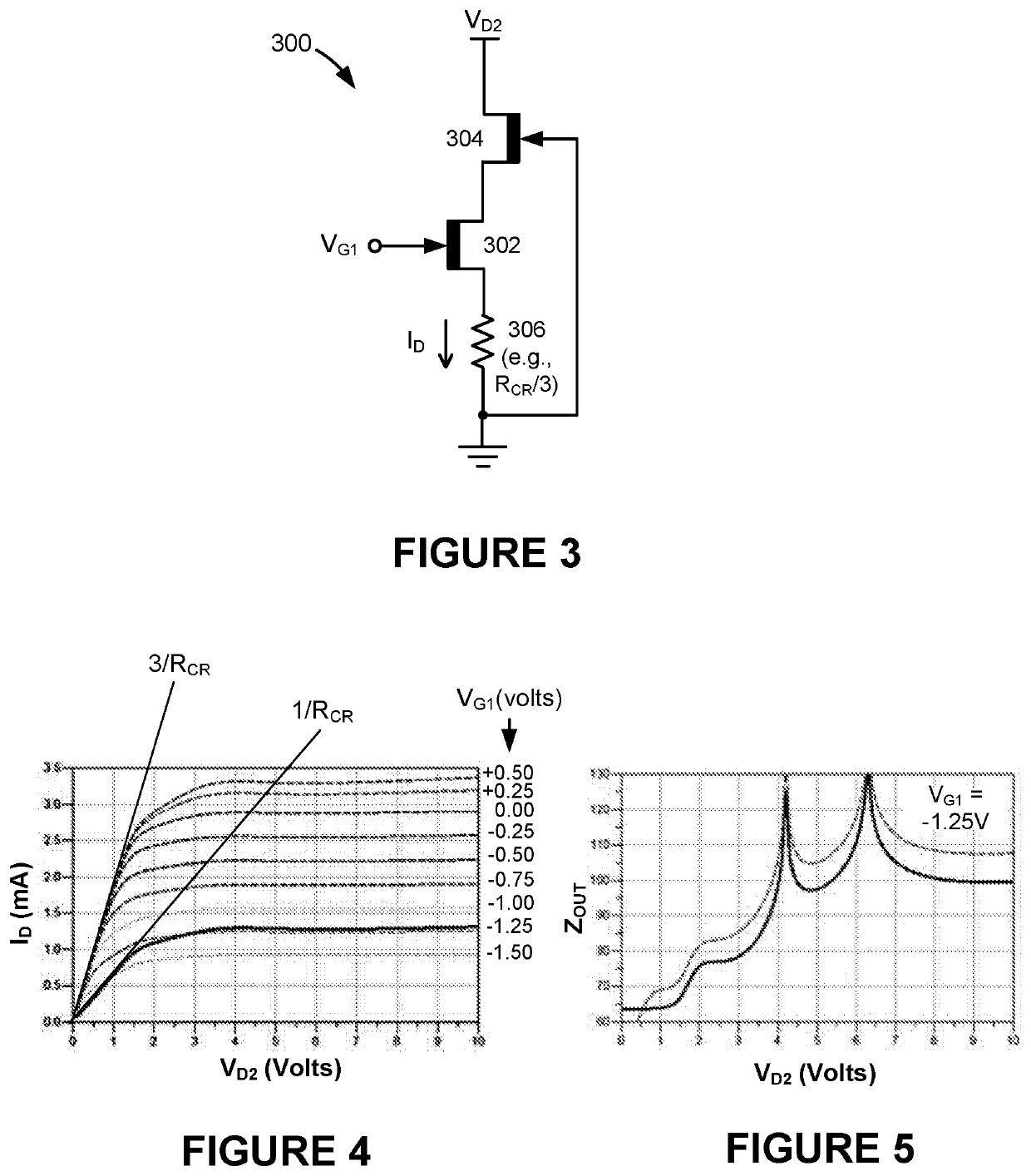
lass="d_n">[0011]Referring to FIG. 3, there is shown a schematic drawing of a voltage controlled adjustable current source 300, according to an embodiment of the present invention. The voltage controlled adjustable current source 300 comprises a first depletion mode field-effect transistor (FET) 302, a second depletion mode FET 304, and a fixed resistor 306. The first depletion mode FET 302 has a drain connected to the source of the second depletion mode FET 304, a source connected to a first terminal of the fixed resistor 306, and a gate configured to receive a current-setting control voltage VG1. The second depletion mode FET 304 has a drain configured to receive a drain voltage VD2, a gate connected to a second terminal of the fixed resistor 306, and a source connected to the drain of the first depletion mode FET 302.

[0012]The voltage controlled adjustable current source 300 is preferably implemented in an integrated circuit (IC), e.g., a monolithic microwave integrated circuit (...


PUM

PropertyMeasurementUnit
voltageaaaaaaaaaa
input drain voltageaaaaaaaaaa
resistanceaaaaaaaaaa

Abstract

A current regulating apparatus capable of regulating an electrical current with a high level of precision and over a wide range of voltages includes a first depletion mode field-effect transistor (FET), a second depletion mode FET, and a fixed resistor. The second depletion mode FET and fixed resistor are connected in series and across the gate-source terminals of the first depletion mode FET. The first depletion mode FET operates as an adjustable current source while the second depletion mode FET is controlled to operate as a voltage controlled resistor. The magnitude of current regulated by the current regulating apparatus is determined based on both the resistance of the fixed resistor and a current-setting control voltage applied to the gate of the second depletion mode FET. Various precision values of regulated current can be realized by simply changing the current-setting control voltage.

Description

BACKGROUND OF THE INVENTION[0001]A current source is an electrical device that maintains a constant current regardless of changes in voltage across it. Current sources can be constructed in various ways. FIG. 1 shows one approach known in the art as a current-regulating diode (or “CR diode”) 100. The CR diode 100 is typically constructed from an n-channel junction field effect transistor (JFET) but may also be constructed from an n-channel depletion mode metal-oxide-semiconductor FET (MOSFET) 102, as in FIG. 1. Both the n-channel JFET and n-channel depletion mode MOSFET are ‘normally ON,’ meaning that they have a negative threshold voltage Vth and can only be turned OFF if their gate-source voltage VGS<Vth. In the CR diode 100 depicted in FIG. 1 the gate-source voltage is VGS=0. Accordingly, so long as the drain voltage VD remains greater than −Vth, the FET 102 remains ON and the CR diode 100 maintains (i.e., regulates) a constant current IDSS proportional to the square of the FE...

Claims


Application Information

Patent Timeline
Patent Type & Authority Patents(United States)
IPC IPC(8): H02M5/293
CPCH02M5/293H02M2005/2932G05F3/247H02M5/2932
Inventor GODYCKI, WACLAW
Owner ERIDAN COMM
Why Eureka
Try Eureka