Method of manufacturing a capacitor

a manufacturing method and capacitor technology, applied in the direction of capacitors, semiconductor devices, electrical devices, etc., can solve the problems of significantly reducing the capacitance of the capacitor, easy collapse of the cylinder-type capacitor, etc., to achieve the effect of improving the capacitance, significantly reducing the plate area of the capacitor, and increasing the plate area

Active Publication Date: 2020-09-22
UNITED MICROELECTRONICS CORP +1
View PDF19 Cites 0 Cited by
  • Summary
  • Abstract
  • Description
  • Claims
  • Application Information

AI Technical Summary

Benefits of technology

[0004]Given that the plate area of capacitor would be significantly decreased in current pillar type capacitor structure, a novel manufacturing method is therefore provided in the present invention, which features the formation of a sidewall with a wave profile to significantly increase the plate area and improve its capacitance.

Problems solved by technology

When current semiconductor technology node is advanced to be smaller than 25 nm, the cylinder-type capacitor would easily suffer collapse issues during processing due to their congenital insufficiency in structural strength.
However, although the pillar-type capacitor solves the collapse issue in prior art, its structural design would lose a large proportion of the plate area in the capacitor and, thereby, significantly lower the capacitance of capacitor.

Method used


Image

  • Method of manufacturing a capacitor
  • Method of manufacturing a capacitor
  • Method of manufacturing a capacitor

Examples


Embodiment Construction

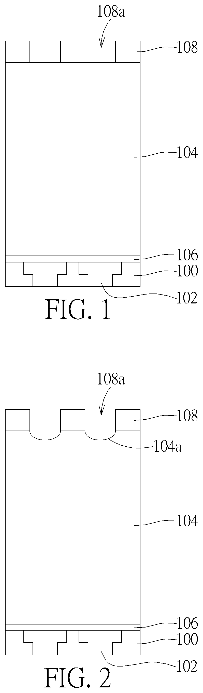
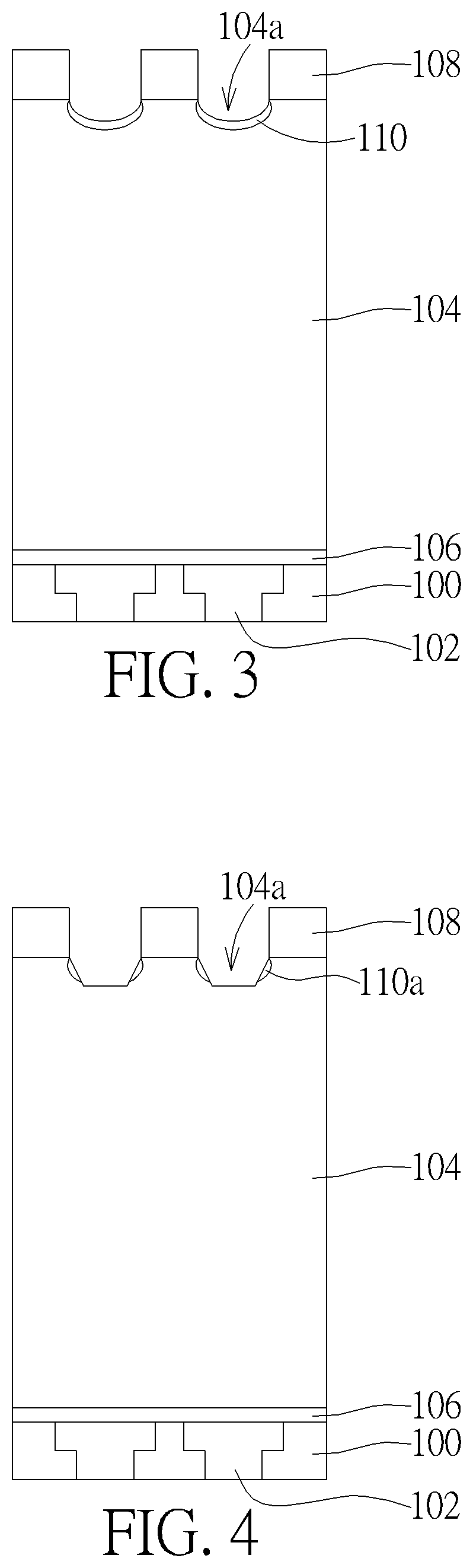
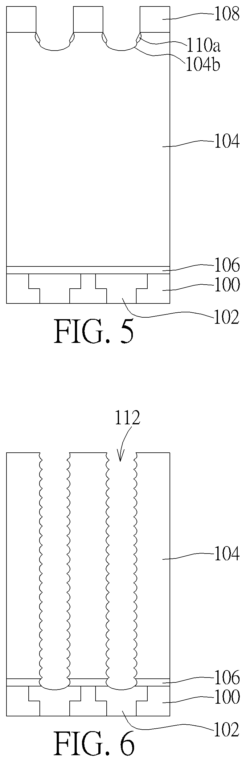
[0010]In the following detailed description of the invention, reference is made to the accompanying drawings, which form a part hereof, and in which is shown, by way of illustration, specific embodiments in which the invention may be practiced. These embodiments are described in sufficient detail to enable those skilled in the art to practice the invention. Other embodiments may be utilized and structural, logical and electrical changes may be made without departing from the scope of the present invention. The following detailed description is, therefore, not to be taken in a limiting sense, and the scope of the present invention is defined only by the appended claims, along with the full scope of equivalents to which such claims are entitled.

[0011]The above description serves to distinguish the term “etching” from “removing.” When etching a material, at least a portion of the material remains behind after the process is completed. In contrast, when removing a material, substantiall...


PUM

PropertyMeasurementUnit
semiconductoraaaaaaaaaa
dielectricaaaaaaaaaa
structural strengthaaaaaaaaaa

Abstract

The present invention discloses a method of manufacturing a capacitor, which includes the steps of forming a capacitor recess in a sacrificial layer, wherein the sidewall of capacitor recess has a wave profile, forming a bottom electrode layer on the sidewall of capacitor recess, filling up the capacitor recess with a supporting layer, removing the sacrificial layer to forma capacitor pillar made up by the bottom electrode layer and the supporting layer, forming a capacitor dielectric layer on the capacitor pillar, and forming a top electrode layer on the capacitor dielectric layer.

Description

BACKGROUND OF THE INVENTION1. Field of the Invention[0001]The present invention generally relates to a method of manufacturing a capacitor, and more specifically, to a method of manufacturing a pillar-type capacitor structure with wave profile.2. Description of the Prior Art[0002]A dynamic random access memory (DRAM) stores one bit of data using one transistor and one capacitor. Because the charge in the capacitor is lost over time, it must be periodically refreshed to maintain the contents stored in the memory, so it is called dynamic. The structure of DRAM is relatively simple, it uses only one transistor and one capacitor to store one bit of data, so its production cost is relatively low. In DRAM architecture, the capacitor is designed to be formed on the memory cell region and connected with the underlying transistor through a capacitor landing pad.[0003]In the evolution of DRAM, the type of capacitor is progressed from early concave-type structure to cylinder-type structure tha...

Claims


Application Information

Patent Timeline
Patent Type & Authority Patents(United States)
IPC IPC(8): H01L27/00H01L49/02H01L27/108
CPCH01L28/87H01L27/10852H01L28/88H01L27/1085H01L28/40H01L28/84H10B12/37H10B12/033H10B12/03
Inventor CHANG, FENG-YILEE, FU-CHE
Owner UNITED MICROELECTRONICS CORP
Why Eureka
Try Eureka