Electrical contact

a technology of electrical contact and current path, applied in the direction of coupling contact member, coupling device connection, coupling/insulating coupling contact member, etc., can solve the problems of limiting the transmission rate of electrical connectors, affecting the high frequency characteristics of conductive terminals, and shortening the current path. , to achieve the effect of improving the high frequency performance of electrical connectors

Active Publication Date: 2020-10-06
FUDING PRECISION COMPONENTS SHENZHEN +1
View PDF32 Cites 7 Cited by
  • Summary
  • Abstract
  • Description
  • Claims
  • Application Information

AI Technical Summary

Benefits of technology

[0004]To achieve the above object, an electrical contact for connecting a chip module to a print circuit board, the electrical contact comprises a main body, an upper elastic arm and a lower mounting arm extending upwardly from the main body, and a lower elastic arm and a lower mounting arm extending downwardly from the main body. The upper mounting arm is disposed at the downside of the upper elastic arm and forms a space therebetween; the lower mounting arm is disposed at the downside of the lower elastic arm and forms a space therebetween. The upper elastic arm and the lower elastic arm are respectively deformed by the chip module and print circuit board to resist to the upper mounting arm and lower mounting arm, thereby shortening the current path between the chip module and the print circuit board for improving the high frequency performance of an electrical connector.

Problems solved by technology

Because of the transmitting speed of the high frequency signal of the electrical connector is continuously require improved, however, the upper and lower elastic arms of such conductive terminals have to be designed in a curved long arm shape due to the abutment demand, which may cause the current path of the conductive terminal becoming very long, thereby affecting its high frequency characteristics and limiting its transmission rate.

Method used


Image

  • Electrical contact
  • Electrical contact
  • Electrical contact

Examples


Embodiment Construction

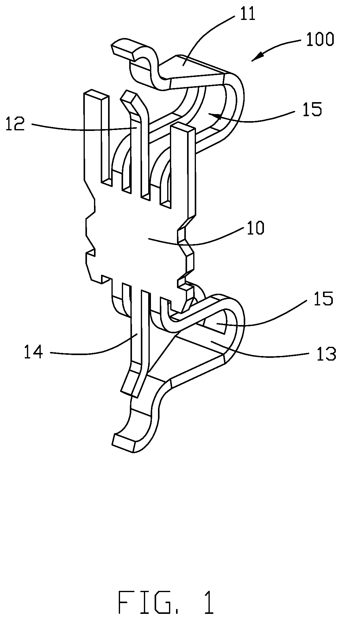
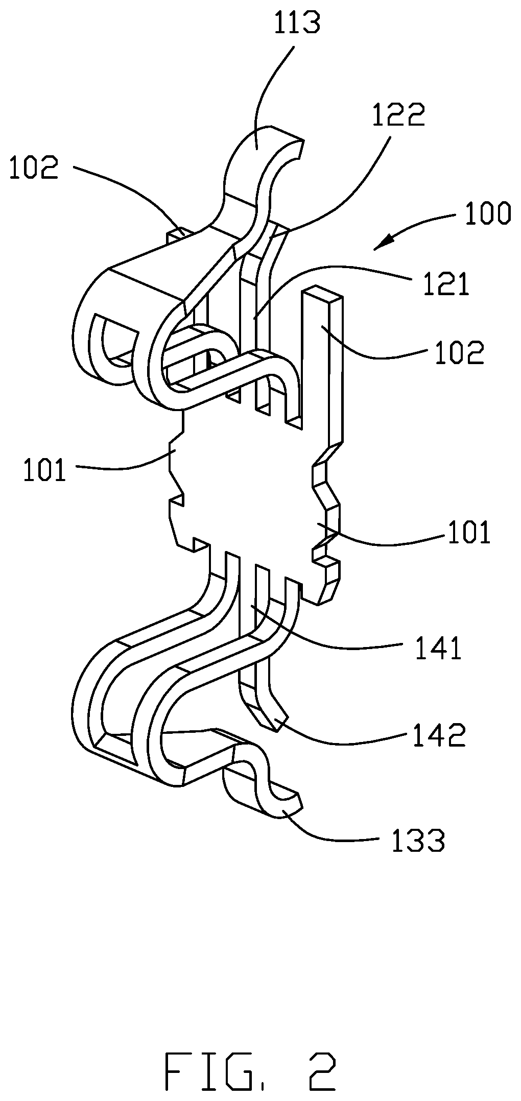
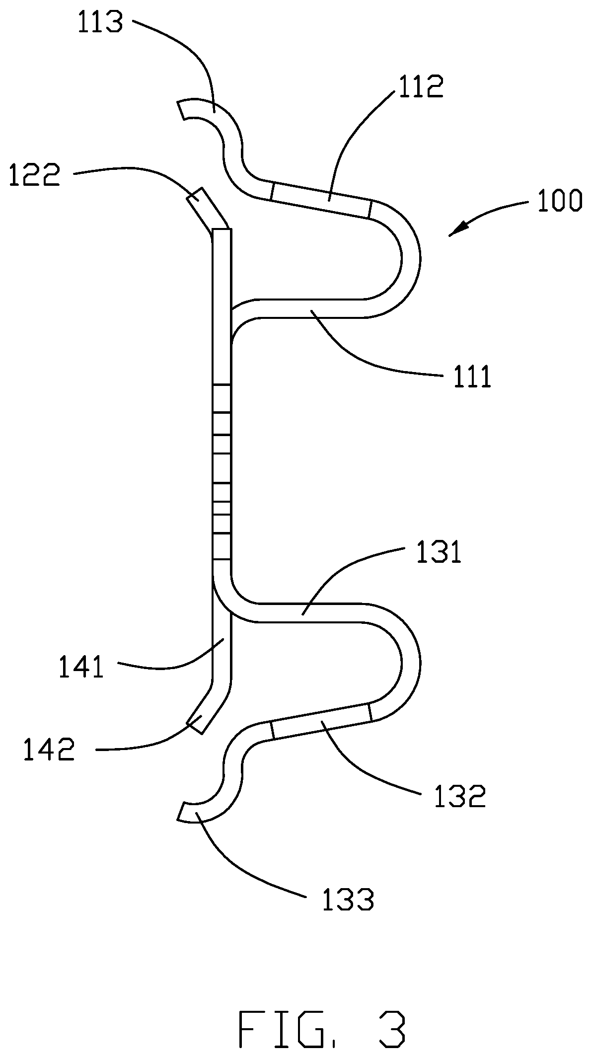
[0019]Referring to FIG. 1-4, an electrical contact 100 for use within an electrical connector to electrically connect a chip module or CPU (Central Processing Unit) 102 to a printed circuit board 101, includes an main body 102, an upper elastic arm 11 and a lower mounting arm 12 extending upwardly from said main body 10, and a lower elastic arm 13 and a lower mounting arm 14 extending downwardly from said main body 10.

[0020]The upper elastic arm (unit) 11 includes a first bending portion 111 extending from the upper end of the main body 10 toward to the direction away from the main body 10, a second bending portion 112 bending upwardly from the first bending portion 111, an arc-shaped upper contacting portion 113 extending upwardly from the second bending portion 112 to the upside of the main body 10; and the lower elastic arm (unit) 13 includes a third bending portion 131 extending from the downside of the main body 10 to the direction away from the main body 10, a forth bending po...


PUM


Abstract

An electrical contact for connecting a chip module to a print circuit board, the electrical contact comprises a main body, an upper elastic arm and a lower mounting arm extending upwardly from the main body, and a lower elastic arm and a lower mounting arm extending downwardly from the main body. The upper mounting arm is disposed at the downside of the upper elastic arm and forms a space therebetween; the lower mounting arm is disposed at the downside of the lower elastic arm and forms a space therebetween. The upper elastic arm and the lower elastic arm are respectively deformed by the chip module and print circuit board to resist to the upper mounting arm and lower mounting arm, thereby shortening the current path between the chip module and the print circuit board for improving the high frequency performance of an electrical connector.

Description

BACKGROUND OF THE INVENTION1. Field of the Invention[0001]The present invention relates generally to an electrical contact, and more particularly to the electrical contact connecting a chip module to a print circuit board.2. Description of Related Arts[0002]U.S. Pat. No. 6,824,396 discloses an electrical connector includes an insulative housing and a conductive terminal, the conductive terminal includes a holding portion mounted to the insulative housing, and an upper elastic arm and a lower elastic arm respectively connected to upper and lower ends of the holding portion. The upper and lower elastic arms are respectively connected the chip module and the print circuit board, when the chip module is pressed to the conductive terminal, the conductive terminal connects the chip module and the circuit board to achieve an electrical conduction. Because of the transmitting speed of the high frequency signal of the electrical connector is continuously require improved, however, the upper ...

Claims


Application Information

Patent Timeline
Patent Type & Authority Patents(United States)
IPC IPC(8): H01R12/00H01R12/71H01R33/74H01R13/646H01R33/94H01R13/24
CPCH01R13/2428H01R13/646H01R33/74H01R33/94H01R13/2435H01R12/714H01R12/7076H01R12/7082H01R13/41
Inventor HSU, SHUO-HSIU
Owner FUDING PRECISION COMPONENTS SHENZHEN
Why Eureka
Try Eureka