Techniques, system and apparatus for selective deposition of a layer using angled ions

a technology of angled ions and selective deposition, applied in the field of device processing, can solve the problems of undue complexity and cost of operation

Active Publication Date: 2020-12-29
VARIAN SEMICON EQUIP ASSOC INC
View PDF12 Cites 5 Cited by
  • Summary
  • Abstract
  • Description
  • Claims
  • Application Information

AI Technical Summary

Benefits of technology

[0042]In sum, the present embodiments provide the advantage of the ability to perform selective deposition of a material on a 3-D structure without the use of a mask. The present embodiments also provide the additional advantage of selectively depositing material in 3-D surfaces while avoiding complex schemes, requiring multiple processing tools.

Problems solved by technology

Present day approaches for selective formation of materials may involve multiple patterning operations, which operations may entail undue complexity and costs.

Method used


Image

  • Techniques, system and apparatus for selective deposition of a layer using angled ions
  • Techniques, system and apparatus for selective deposition of a layer using angled ions
  • Techniques, system and apparatus for selective deposition of a layer using angled ions

Examples


Embodiment Construction

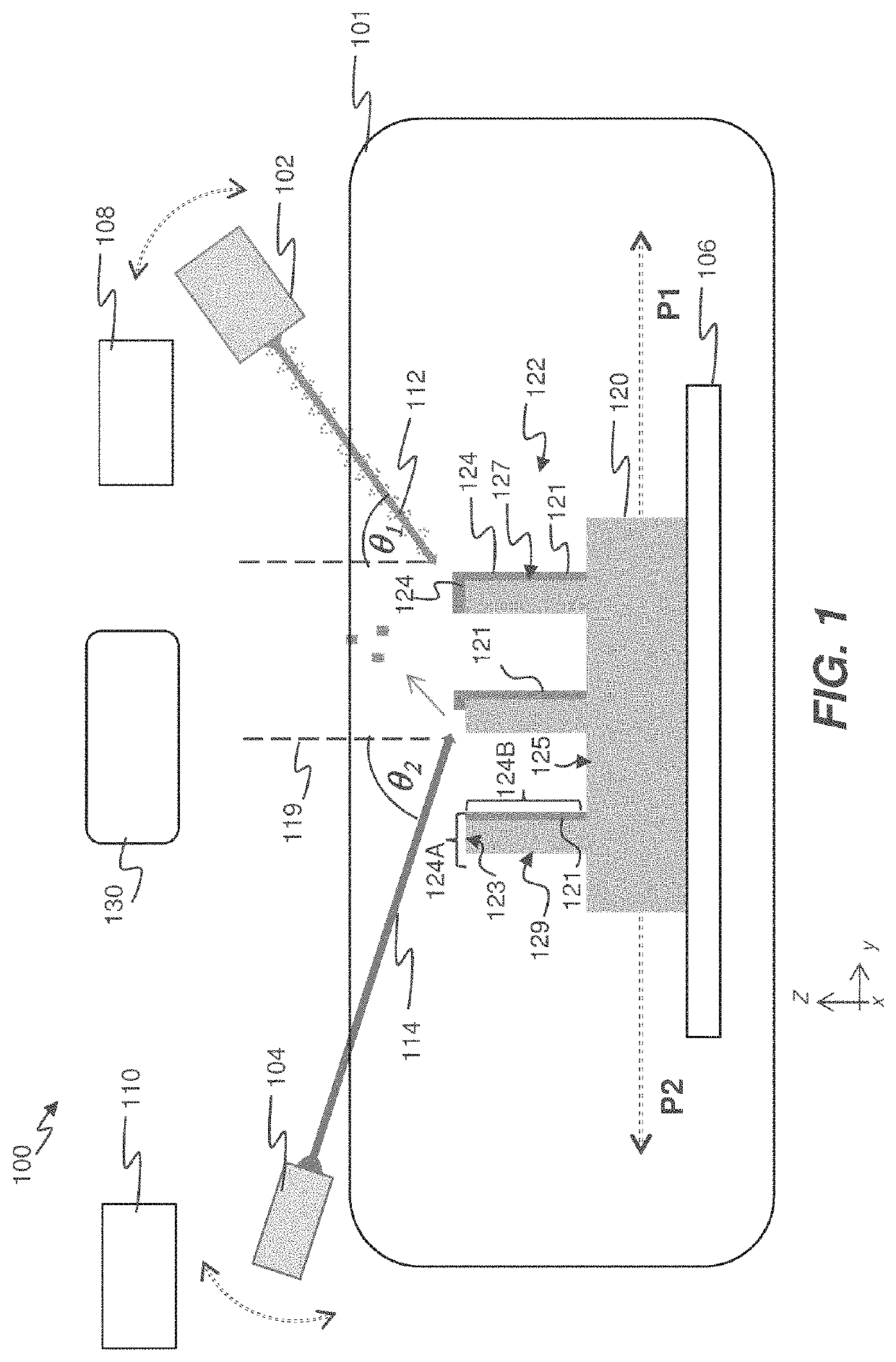
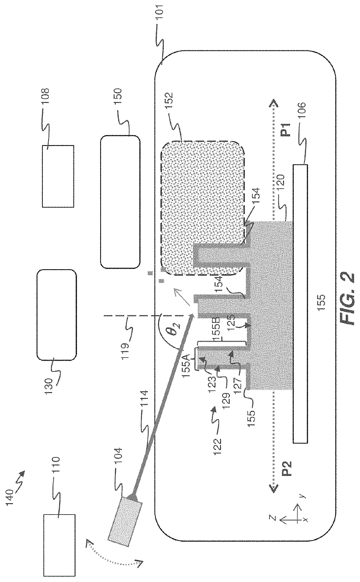
[0014]The present embodiments will now be described more fully hereinafter with reference to the accompanying drawings, where some embodiments are shown. The subject matter of the present disclosure may be embodied in many different forms and are not to be construed as limited to the embodiments set forth herein. These embodiments are provided so this disclosure will be thorough and complete, and will fully convey the scope of the subject matter to those skilled in the art. In the drawings, like numbers refer to like elements throughout.

[0015]In accordance with some embodiments, novel approaches for selectively forming a layer on a substrate, and in particular, novel approaches are provided for building device structures using selective formation of a layer, facilitated by angled ions. In various embodiments selective formation of a layer is accomplished using a combination of operations, including a deposition source for deposition of a layer, and an angled ion source for selective...


PUM

PropertyMeasurementUnit
ion energyaaaaaaaaaa
relative angle of incidenceaaaaaaaaaa

Abstract

A method is provided. The method may include providing a substrate, the substrate comprising a substrate surface, the substrate surface having a three-dimensional shape. The method may further include directing a depositing species from a deposition source to the substrate surface, wherein a layer is deposited on a deposition region of the substrate surface. The method may include performing a substrate scan during the directing or after the directing to transport the substrate from a first position to a second position. The method may also include directing angled ions to the substrate surface, in a presence of the layer, wherein the layer is sputter-etched from a first portion of the deposition region, and wherein the layer remains in a second portion of the deposition region.

Description

FIELD[0001]The present embodiments relate to device processing, and more particularly, to selective deposition of a given material on a substrate.BACKGROUND[0002]In the present day, semiconductor and other devices are scaled to smaller and smaller sizes, where such devices may be formed of many different materials, having complex structures, often arranged in multiple different layers on a substrate. One approach to address the increasing complexity of materials and device structures is selective formation of a given material on selected portions of a device structure, which approach may be especially useful to address patterning issues of a device at the micrometer level or nanometer level. Present day approaches for selective formation of materials may involve multiple patterning operations, which operations may entail undue complexity and costs.[0003]With respect to these and other considerations the present disclosure is provided.BRIEF SUMMARY[0004]In one embodiment, a method is...

Claims


Application Information

Patent Timeline
Patent Type & Authority Patents(United States)
IPC IPC(8): H01J37/34H01J37/32C23C14/34C23C14/58H01L21/263H01L21/285H01L21/02
CPCC23C14/34H01J37/32715H01J37/3464C23C14/5873H01L21/2633H01J37/32376H01J2237/1505H01L21/02631H01J2237/334H01L21/02266H01J2237/20221H01J2237/332H01L21/2855H01L21/3065H01L21/31116H01L21/32136H01L21/76825H01L21/76816H01L21/76813H01L21/67017H01L21/67276H01L21/67213
Inventor HATEM, CHRISTOPHERANGLIN, KEVIN
Owner VARIAN SEMICON EQUIP ASSOC INC
Why Eureka
Try Eureka