Supercharge Your Innovation With Domain-Expert AI Agents!

Low noise bit line circuits

a bit line circuit and low noise technology, applied in information storage, static storage, instruments, etc., can solve problems such as affecting sensing margins and noise across the pag

Active Publication Date: 2021-01-05
MACRONIX INT CO LTD
View PDF11 Cites 1 Cited by
  • Summary
  • Abstract
  • Description
  • Claims
  • Application Information

AI Technical Summary

Benefits of technology

The solution effectively reduces noise across the page, maintaining stable bit line voltages and improving sensing margins, thereby enhancing the operational reliability and accuracy of high-density memory devices.

Problems solved by technology

As the density of memory devices increases, these variations in voltages can induce noise across the page that impacts sensing margins.

Method used


Image

  • Low noise bit line circuits
  • Low noise bit line circuits
  • Low noise bit line circuits

Examples


Embodiment Construction

[0016]A detailed description of embodiments of the present invention is provided with reference to the FIGS. 1-6. Sample implementations are described to illustrate the technology disclosed, not to limit its scope, which is defined by the claims. Those of ordinary skill in the art will recognize a variety of equivalent variations on the description that follows.

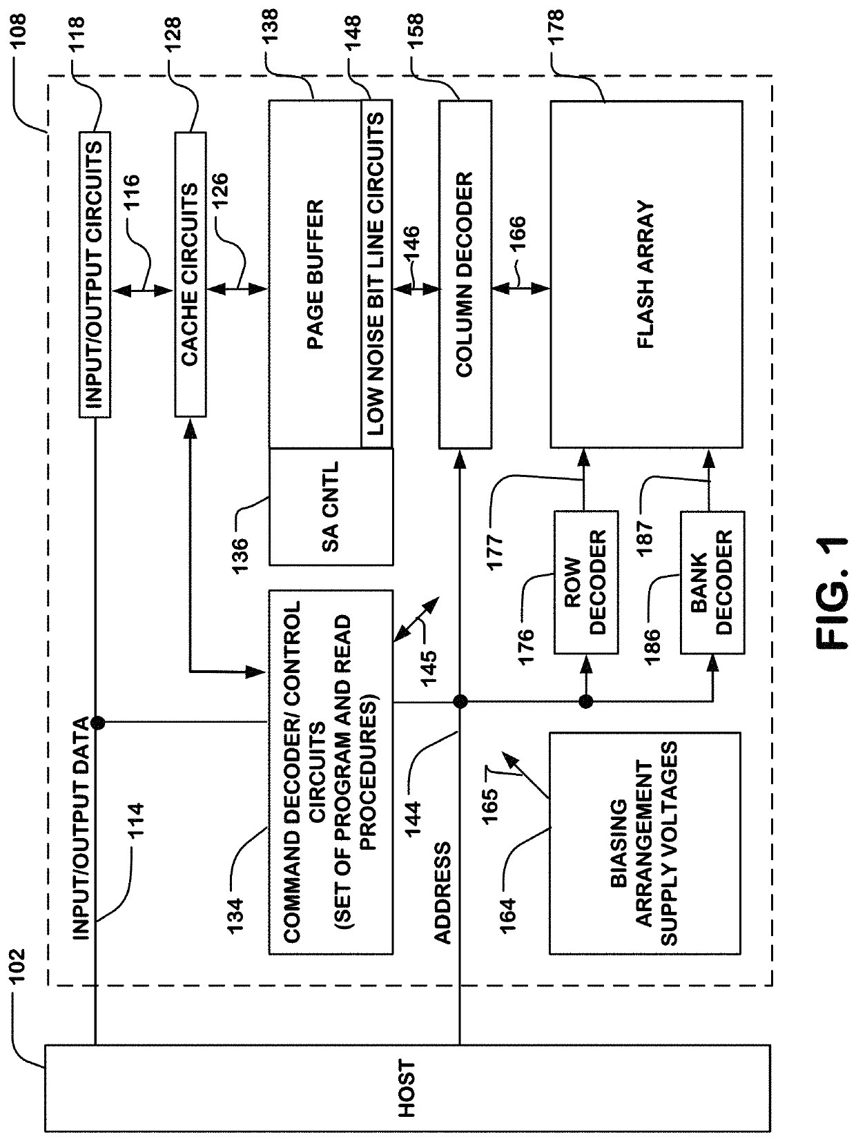
[0017]FIG. 1 is a simplified diagram of a memory system that includes a flash memory device 108 implemented on an integrated circuit and a host 102 configured for page operations, or other operations that include reading a plurality of cells in parallel. The example memory system includes logic for page reading and programming with sense amplifiers and control circuits as described herein. In various embodiments, the memory device 108 may have single-level cells (SLC), or multiple level cells storing more than one bit per cell (e.g., MLC, TLC or XLC). The memory device can be implemented on a single integrated circuit chip, o...


PUM


Abstract

The disclosed technology teaches a memory device with memory cells, each with a sense circuit with an input node in current flow communication, a BLC transistor, a transfer transistor, a current source transistor, and an output circuit to generate data based on a voltage on the sensing node. Also disclosed is a sensing sequence in which control circuits apply BLC voltage to the BLC transistor, transfer voltage to the transfer transistor and current control voltage to the current source transistor to provide a charging current to the BL, and to adjust the current control voltage to provide a keeping current on the BL from the current source transistor, and to apply a read voltage to a selected memory cell on the bit line. Additionally included is applying a timing signal to the output circuit to generate the data based on a voltage on the sensing node.

Description

BACKGROUNDField of the Technology[0001]The present disclosure relates to high density memory devices, in which bit line charging current used during operation of the devices is controlled.Description of Related Art[0002]NAND flash memory is widely adopted as a storage medium for mobile devices, solid-state disks in laptops and servers and for other data processing systems. As the data density on NAND flash memory chips has increased, page operations have become prevalent, in which large numbers of bit lines are used in parallel for access to the memory cells of a page of data. Other memory architectures also provide for parallel sensing operations using large numbers of bit lines.[0003]The data pattern in a page read can vary widely and, as a result, the voltages on the bit lines and sensing circuits varies across the page. As the density of memory devices increases, these variations in voltages can induce noise across the page that impacts sensing margins.[0004]It is desirable, the...

Claims


Application Information

Patent Timeline
Patent Type & Authority Patents(United States)
IPC IPC(8): G11C16/24G11C16/26
CPCG11C16/24G11C16/26G11C16/32G11C2207/002
Inventor HUNG, JI-YU
Owner MACRONIX INT CO LTD
Features
  • R&D
  • Intellectual Property
  • Life Sciences
  • Materials
  • Tech Scout
  • Unparalleled Data Quality
  • Higher Quality Content
  • 60% Fewer Hallucinations
Learn More