Image intensifier for night vision device

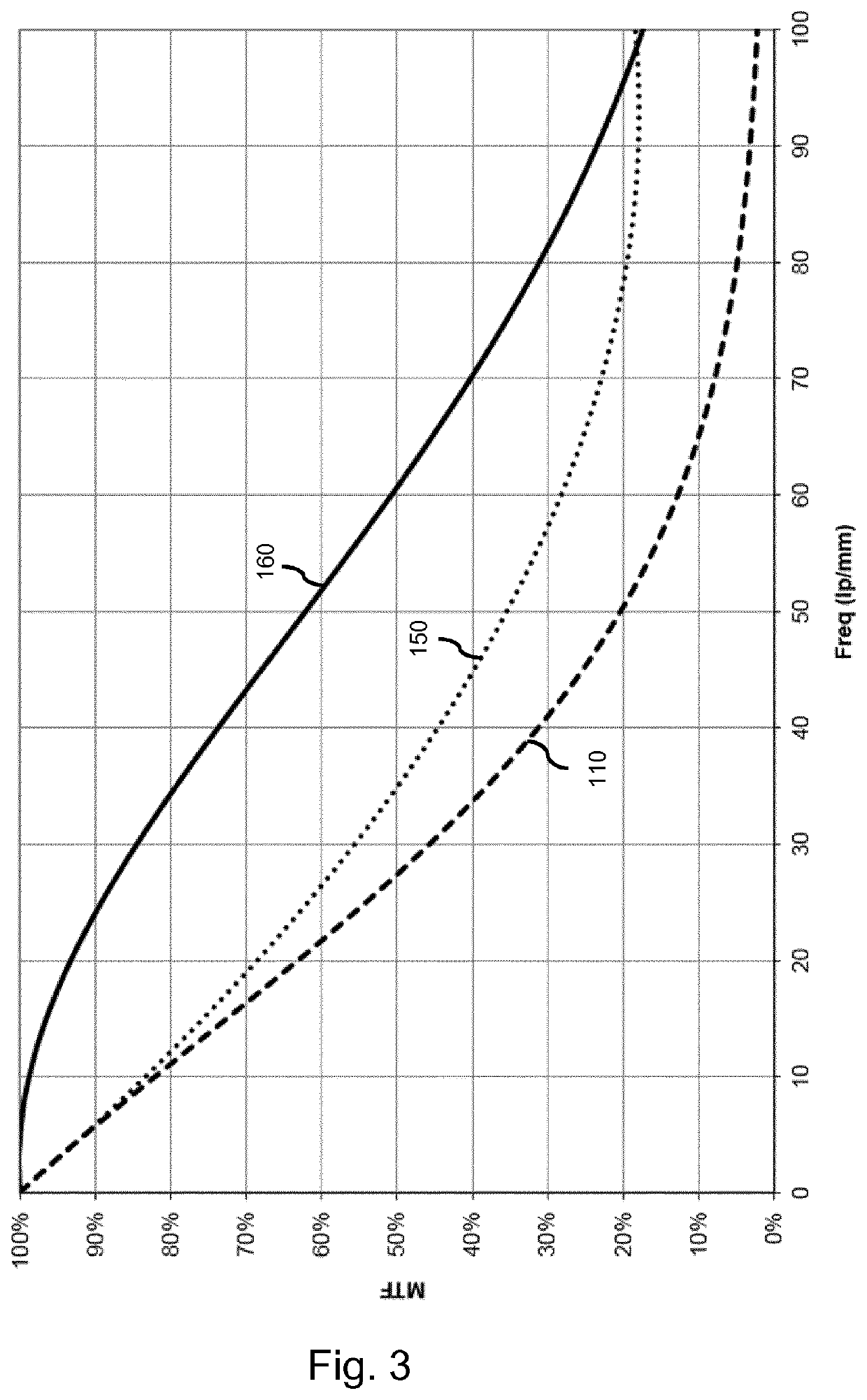
a technology of image intensifier and night vision, which is applied in the direction of multiplier electrode arrangement, instrument, electric multiplier tube, etc., can solve the problem of low image quality of visible image on the phosphorous screen, e.g., as characterized by a mtf, and achieve the effect of improving image quality

Active Publication Date: 2021-01-05
PHOTONIS NETHERLANDS
View PDF12 Cites 0 Cited by
  • Summary
  • Abstract
  • Description
  • Claims
  • Application Information

AI Technical Summary

Benefits of technology

[0013]One of the objects of the invention is to provide an image intensifier having an improved image quality, e.g., as characterized by a MTF.
[0023]The inventor(s) have further recognized a reason for the anode gap being such a major factor in reducing the overall MTF of the image intensifier. Namely, as can be seen in FIG. 5, which shows one MCP channel and a number of trajectories of electrons leaving the MCP channel and entering the field between the MCP and the anode, when an electron leaves the center of the MCP channel without any radial speed, it would be accelerated directly towards the projected point on the anode screen. However, the electrons leaving the MCP channel may have a wide energy distribution, e.g., between 0-300V, and may have a wide angular distribution. In addition, the change in electrical field between the MCP channel and the anode gap may effectively establish an electrostatic lens. This electrostatic lens may add a further radial velocity component to electrons leaving the MCP channel. Here, the term radial velocity component refers to the velocity component orthogonal to the straight line between MCP channel and anode. Since the size and direction of this radial velocity components varies due to the aforementioned reasons, the electrons leaving one particular MCP channel of the MCP may be distributed over a certain area on the anode, thereby causing the anode to produce a blurry spot in visible light.
[0026]By introducing the thin film in the image intensifier, the cloud of electrons emitted from the electron multiplier may be released into the thin film. Due to the characteristics of the thin film, a number of electrons may drift through the thin film towards the electron transmitting side and escape the thin film. The latter may be supported by the electron transmitting side having a negative electron affinity. The thickness of the thin film is chosen to result in the electrons losing at least a substantial part of their excess energy and thereby floating on the conduction band. Effectively, the electrons may become thermalized electrons. Accordingly, the electrons leaving the thin film may have low energy and a small energy distribution (e.g., less than 1 eV). The electrons leaving the film may thus cross the anode gap with little radial velocity. An advantage of having little radial velocity is that the electrons may travel more along a straight line towards the anode. Accordingly, blurry spots on the anode may be reduced in size or substantially avoided. The MTF of the anode gap may thus improve. Advantageously, the overall MTF of the image intensifier may improve.
[0027]Optionally, the thin film consists of an electron energy absorption layer at the electron receiving side of the thin film and an exit layer at the electron emitting side of the thin film, wherein the exit layer comprises the surface having the negative electron affinity. The electron energy absorption layer may be selected to comprise the (poly) crystalline structure having the desired band gap and the desired carrier diffusion length. The electron energy absorption layer may thus effectively provide the ‘bulk’ to absorb and thermalize the electrons, while the exit layer, which may be a relatively thin layer, may provide the negative electron affinity at the electron emitting side.
[0040]Optionally, the surface of the thin film at the electron receiving side has a positive electron affinity. A positive electron affinity may help avoid re-emitting the trapped electrons to the vacuum on the electron receiving side of the thin film.
[0041]Optionally, an electric field is applied across the thin film so as to facilitate migration of electrons from the electron receiving side to the electron emitting side. An electric field may help electrons to migrate to the surface at the electron emitting side.

Problems solved by technology

A problem of known image intensifiers is that the image quality of the visible image on the phosphorous screen, e.g., as characterized by a MTF, is too low.

Method used


Image

  • Image intensifier for night vision device
  • Image intensifier for night vision device
  • Image intensifier for night vision device

Examples


Embodiment Construction

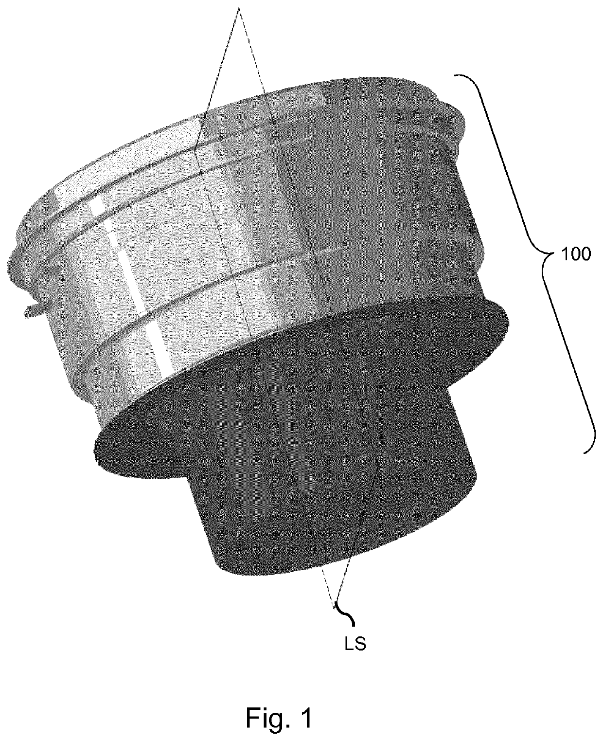
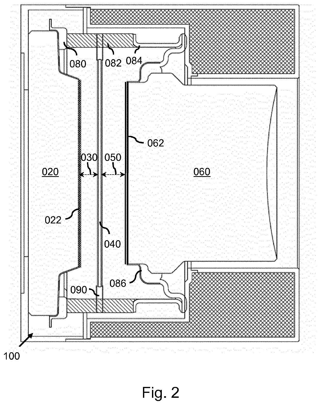
[0079]FIGS. 1 and 2 show an image intensifier in the form of an image intensifier (I2) tube 100. The I2 tube as shown is known per se from the field of night vision devices, and is used in the following as a non-limiting example of an image intensifier.

[0080]Indicated in FIG. 1 is a longitudinal plane LS. FIG. 2 shows a longitudinal section of the I2 tube 100 along this plane LS. It can be seen that the I2 tube 100 comprises an input lens 020 with a photosensitive layer 022 forming a photocathode (henceforth referred to as photocathode 022, or in short cathode), an electron multiplier 040 in the form of a micro channel plate, and a phosphorous screen 062 on top of a glass- or fiber-optic output lens 060 acting as an anode (and henceforth also simply referred to as anode). Further illustrated in FIG. 2 are, by way of dashed arrows, the cathode gap 030, referring to the input gap or channel between the photocathode 022 and the electron multiplier 040, as well as the anode gap 050, ref...


PUM

PropertyMeasurementUnit
band gapaaaaaaaaaa
diffusion lengthaaaaaaaaaa
thicknessaaaaaaaaaa

Abstract

An image intensifier is provided in which a thin film (090) is arranged between an output surface of the electron multiplier (040) and the phosphorous screen. The thin film is a semi-conductor or insulator with a crystalline structure comprising a band gap equal or larger than 1 eV, wherein the crystalline structure has a carrier diffusion length equal or larger than 50% of the thickness of the thin film. In addition, the thin film has an anode directed surface which has a negative electron affinity. By way of provisioning a thin film of the above type in the image intensifier, an improvement in mean transfer function of the overall image intensifier is obtained.

Description

[0001]This application is the U.S. national phase of International Application No. PCT / EP2017 / 050278 filed 6 Jan. 2017, which designated the U.S. and claims priority to EP Patent Application No. 16150579.7 filed 8 Jan. 2016, the entire contents of each of which are hereby incorporated by reference.FIELD OF THE INVENTION[0002]The invention relates to an image intensifier for obtaining an intensified display of a scene. The invention further relates to a night vision device comprising the image intensifier, and to a head mount, a weapon sight or a handheld device comprising the night vision device.BACKGROUND ART[0003]Night vision devices are direct view systems which comprise image intensifiers for obtaining an intensified display of a scene. Such night vision devices are frequently head-, helmet- or weapon-mounted, and may optionally include an optical or digital overlay of images from a parallel line-of-sight infrared camera, data from a GPS or compass system, etc. The image intensi...

Claims


Application Information

Patent Timeline
Patent Type & Authority Patents(United States)
IPC IPC(8): H01L31/00G02B23/12H01J31/50H01J43/24
CPCH01J31/507G02B23/12H01J31/50H01J43/246H01J2231/5016
Inventor NÜTZEL, GERT OTTO
Owner PHOTONIS NETHERLANDS
Why Eureka
Try Eureka