AM-EWOD circuit configuration with sensing column detection circuit

a technology of sensing column and circuit configuration, which is applied in the field of amewod circuit configuration with sensing column detection circuit, can solve the problems of limiting the extent to which the array element can be made smaller, the actual system is impractical for real-word device applications, and the experimental use of such external components is impractical for large arrays, so as to achieve sufficient integration, enhance balance, and reduce the size of the array elemen

Active Publication Date: 2021-04-13
SHARP LIFE SCI EU LTD
View PDF10 Cites 0 Cited by
  • Summary
  • Abstract
  • Description
  • Claims
  • Application Information

AI Technical Summary

Benefits of technology

[0029]There is a need in the art to provide a thin film electronics configuration for an AM-EWOD device that provides an enhanced balance between the advantages of an integrated sensing capability and the desire for a small array element size. This disclosure describes an integrated impedance sensing arrangement within the thin film electronics structure, whereby sensing can be implemented without providing additional circuit components specifically within the array element structure itself. Such a configuration achieves sufficient integration to keep a small number of connections to the thin film electronics substrate without enlargement of individual array element circuitry, and without using external sensing devices that are not suitable for large arrays of hundreds or even thousands of columns.
[0035]An advantage of the embodiments over conventional configurations is that sensing the capacitance present at each array element in the device array is performed without requiring additional circuit elements to be integrated specifically into the array element circuitry. There remains substantial sensing integration, however, as the sensing function is integrated into the column detection circuit within the thin film electronics layer. In this manner, substantial benefits of integrated sensing are achieved, such as for example closed loop functioning and high signal-to-noise ratio, without having to increase the size of the array element circuitry in each individual array element as desired for high resolution applications.

Problems solved by technology

Although providing an experimental basis for such mutual capacitance sensing, the actual system is impractical for real-word device applications.
The experimental usage of such external components is impractical for large arrays since an external connection is needed to each column of the array.
While this affords good performance sensing with a high signal-to-noise ratio, the additional circuit components add real estate and limit the extent to which the array elements can be made smaller.

Method used


Image

  • AM-EWOD circuit configuration with sensing column detection circuit
  • AM-EWOD circuit configuration with sensing column detection circuit
  • AM-EWOD circuit configuration with sensing column detection circuit

Examples


Embodiment Construction

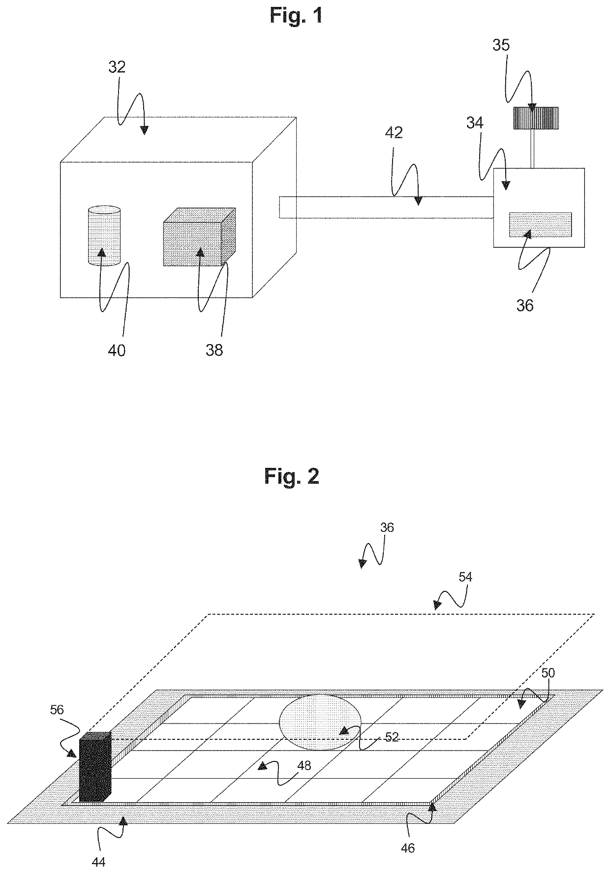
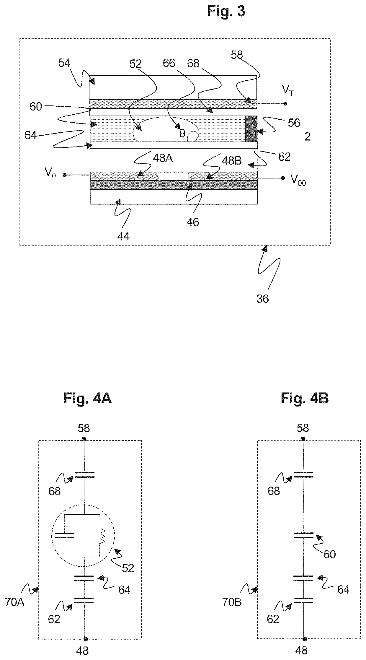
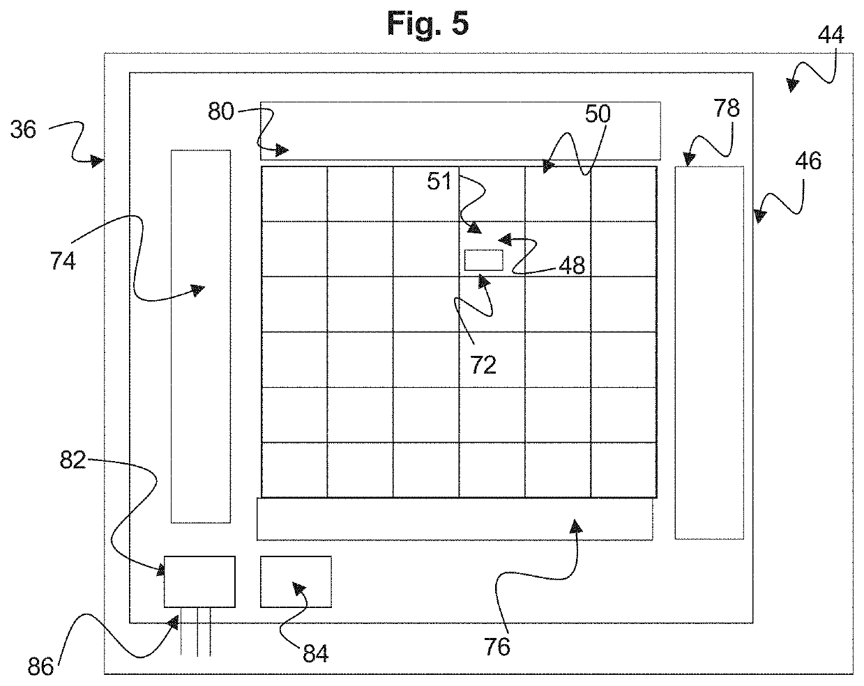
[0058]Embodiments of the present invention will now be described with reference to the drawings, wherein like reference numerals are used to refer to like elements throughout. It will be understood that the figures are not necessarily to scale.

[0059]FIG. 8 is a drawing depicting a circuit representation of components of a portion of an AM-EWOD device 100, which may have a structural configuration comparably as depicted in FIGS. 1-5. In this illustration, the device portion 100 spans two array elements including a first array element electrode 102 and a second array element electrode 104. For applying actuation voltages, the array element electrodes 102 and 104 are spaced apart from a reference (top) electrode 106, whereby actuation voltages are applied based on a potential difference between the array element electrodes and the reference electrode. CI represents the series capacitance combination of an ion barrier insulator 108 and a first hydrophobic coating 110 applied on the arra...


PUM

PropertyMeasurementUnit
electrowetting voltagesaaaaaaaaaa
actuation voltageaaaaaaaaaa
voltageaaaaaaaaaa

Abstract

An AM-EWOD device includes a plurality of array elements arranged in an array of rows and columns; each column including a column addressing line that applies control signals to a corresponding column of array elements, and each row including a row addressing line that applies control signals to a corresponding row of array elements; each array element including an element electrode for receiving an actuation voltage and a switch transistor, wherein the switch transistor is electrically connected between the column addressing line and the element electrode and is switched by the row addressing line; and a column detection circuit comprising an addressing circuit that applies an electrical perturbation during a sensing operation to the column addressing line of an array element being sensed, and a measuring circuit that measures an output signal from one of the column addressing lines, wherein the output signal varies based upon a capacitance present at the element electrode.

Description

TECHNICAL FIELD[0001]The present invention relates to droplet microfluidic devices, and more specifically to Active Matrix Electrowetting-On-Dielectric (AM-EWOD) devices and to circuit configurations of such devices that employ column based sensing to optimize sensing capabilities as balanced against the desire for a compact arrangement.BACKGROUND ART[0002]Electrowetting on dielectric (EWOD) is a well-known technique for manipulating droplets of fluid by application of an electric field. Active Matrix EWOD (AM-EWOD) refers to implementation of EWOD in an active matrix array incorporating transistors, for example by using thin film transistors (TFTs). It is thus a candidate technology for digital microfluidics for lab-on-a-chip technology. An introduction to the basic principles of the technology can be found in “Digital microfluidics: is a true lab-on-a-chip possible?”, R. B. Fair, Microfluid Nanofluid (2007) 3:245-281).[0003]FIG. 1 is a drawing depicting an exemplary EWOD based mic...

Claims


Application Information

Patent Timeline
Patent Type & Authority Patents(United States)
IPC IPC(8): G01N27/26G09G3/34B01L3/00G02B26/00G09G3/00G01N27/02G01R27/22
CPCG09G3/348B01L3/50273B01L3/502792G01N27/028G01R27/22G02B26/005G09G3/006B01L3/5027B01L2200/0673B01L2200/12B01L2200/143B01L2300/0645B01L2300/089B01L2300/161B01L2400/0427
Inventor HADWEN, BENJAMIN JAMESBEARD, OLIVER JAMESBROWN, CHRISTOPHER JAMES
Owner SHARP LIFE SCI EU LTD
Why Eureka
Try Eureka