

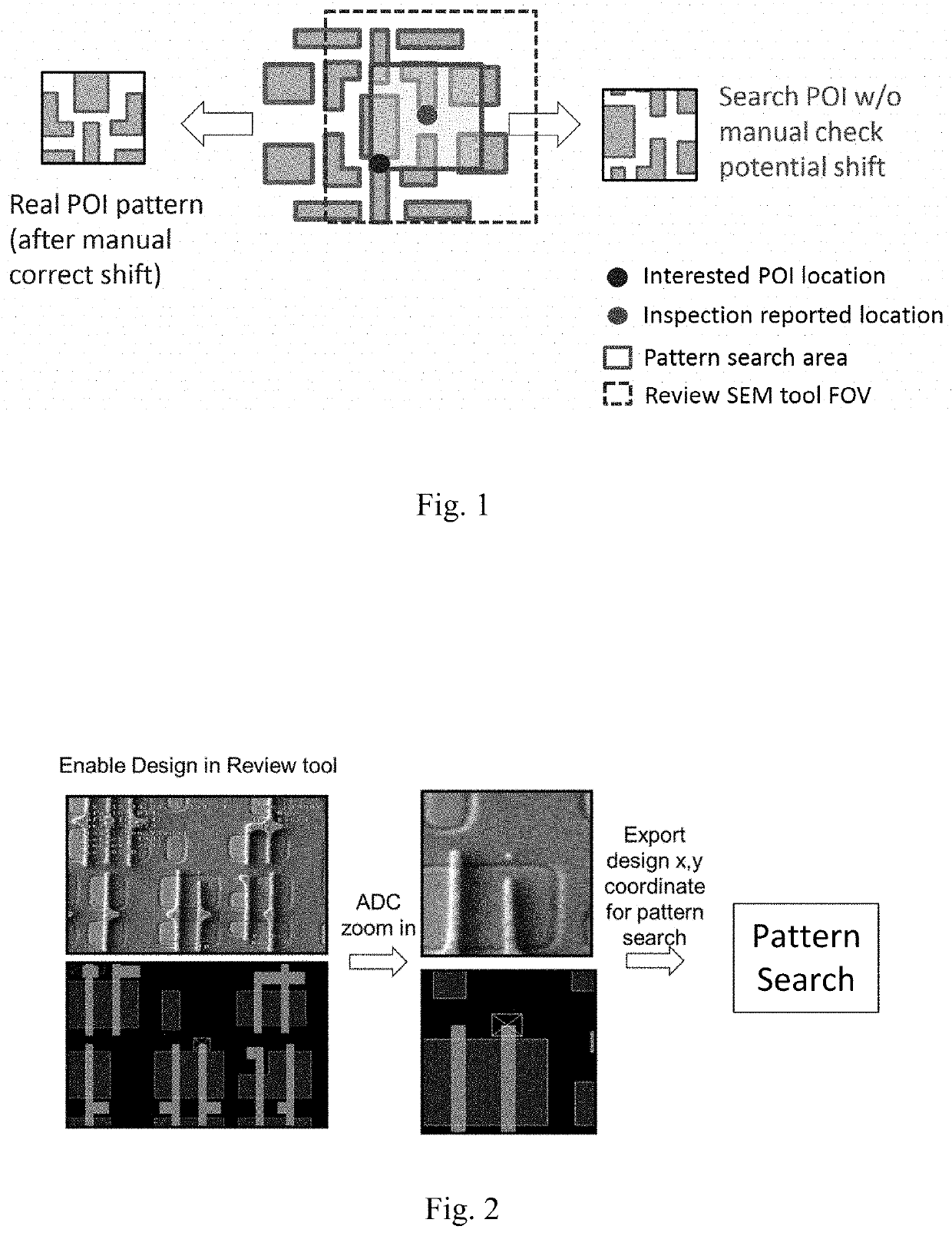
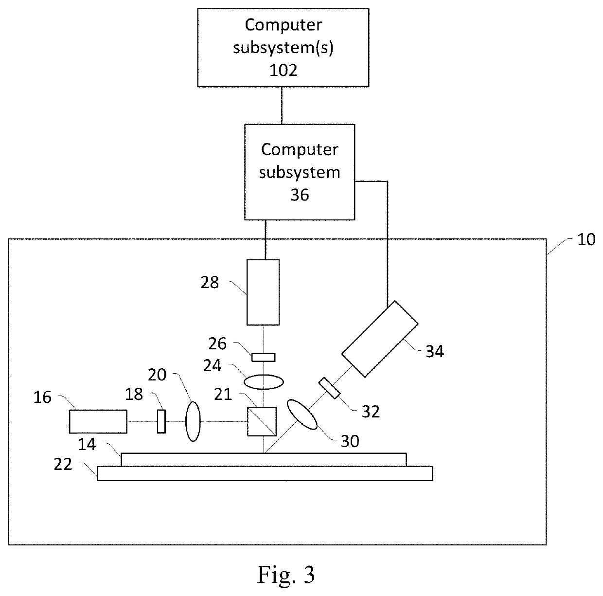
Systems and methods for automatic correction of drift between inspection and design for massive pattern searching
a technology of automatic correction and drift detection, applied in the field of defect detection, can solve the problems of affecting the electrical parameters of the device, the operation of the semiconductor manufacturing process closer to the limitation of the performance capability of the process, and the failure to detect defects of decreasing siz
- Summary
- Abstract
- Description
- Claims
- Application Information
AI Technical Summary
Benefits of technology
Problems solved by technology
Method used
Image

Examples
Embodiment Construction
[0035]Although claimed subject matter will be described in terms of certain embodiments, other embodiments, including embodiments that do not provide all of the benefits and features set forth herein, are also within the scope of this disclosure. Various structural, logical, process step, and electronic changes may be made without departing from the scope of the disclosure. Accordingly, the scope of the disclosure is defined only by reference to the appended claims.
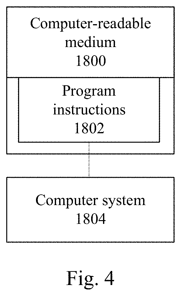
[0036]As used herein, the term “wafer” generally refers to substrates formed of a semiconductor or non-semiconductor material. Examples of such a semiconductor or non-semiconductor material include, but are not limited to, monocrystalline silicon, gallium arsenide, and indium phosphide. Such substrates may be commonly found and / or processed in semiconductor fabrication facilities.
[0037]A wafer may include one or more layers formed upon a substrate. For example, such layers may include, but are not limited to, a resist, a ...
PUM
| Property | Measurement | Unit |
|---|---|---|
| scanning electron microscopy | aaaaa | aaaaa |
| SEM | aaaaa | aaaaa |
| automatic defect | aaaaa | aaaaa |
Abstract
Description
Claims
Application Information