Method of selective silicon germanium epitaxy at low temperatures

a silicon germanium and low temperature technology, applied in the direction of polycrystalline material growth, crystal growth process, chemically reactive gas, etc., can solve the problems of reducing the epitaxy growth of silicon germanium, reducing the growth selectivity of si over dielectric materials, and reducing the deposition or growth selectivity of si

Active Publication Date: 2021-05-25
APPLIED MATERIALS INC
View PDF15 Cites 171 Cited by
  • Summary
  • Abstract
  • Description
  • Claims
  • Application Information

AI Technical Summary

Problems solved by technology

During such processes, the temperature of the substrate is increased to, and / or maintained at, temperatures above 500° C. However, at substrate temperatures below 500° C., epitaxial growth of silicon germanium diminishes and deposition or growth selectivity for Si over dielectric materials drastically decreases.

Method used


Image

  • Method of selective silicon germanium epitaxy at low temperatures
  • Method of selective silicon germanium epitaxy at low temperatures
  • Method of selective silicon germanium epitaxy at low temperatures

Examples


Embodiment Construction

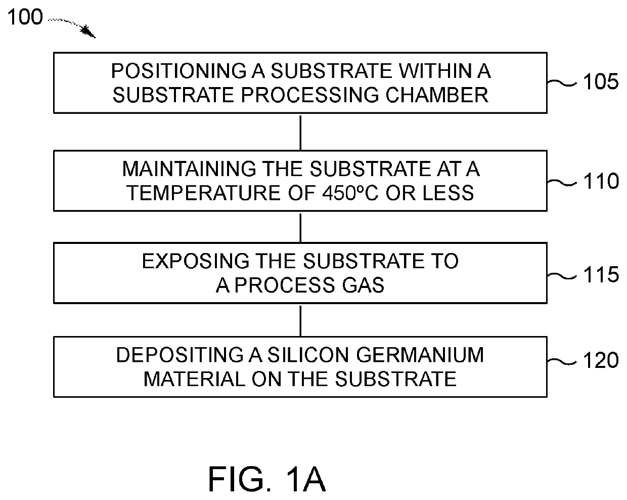
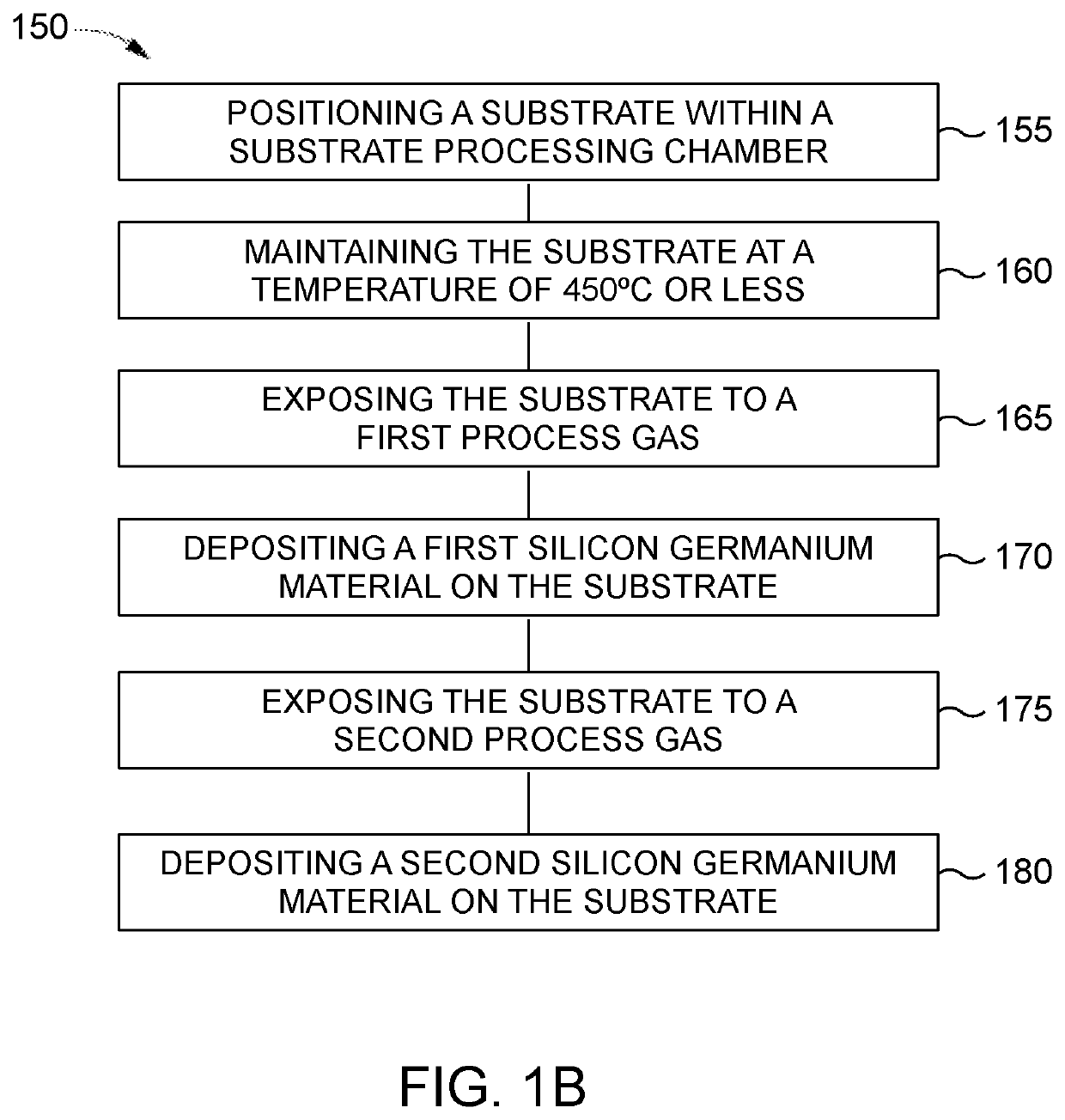
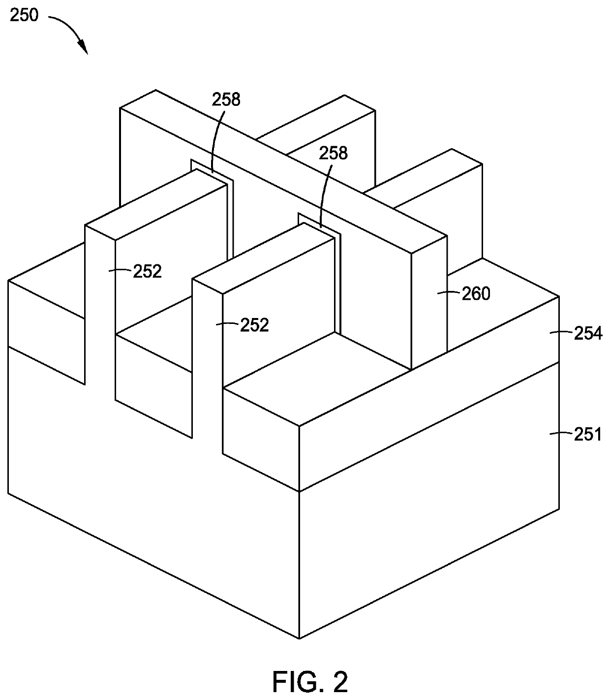
lass="d_n">[0018]Embodiments described herein illustrate a process to epitaxially deposit silicon containing compounds during the manufacture of various device structures. The processes described herein allow for selective and epitaxial growth or deposition of a silicon germanium film layer on exposed crystalline silicon containing regions of a substrate and not on exposed dielectric regions of the substrate, at low substrate temperatures (e.g., about 450° C. or less), with almost complete selectivity for the exposed crystalline silicon over the exposed dielectric of the substrate, when performed at temperatures of about 400° C., such as about 350° C. or less. The processes herein advantageously provide boron concentrations in the grown or deposited silicon containing compound of about 1×10¹⁵ or greater, such as about 1×10²¹ or greater, such as about 5×10²¹. Moreover, the dopant, such as boron, advantageously allows growth or deposition of epitaxial silicon germanium materials at lo...


PUM

PropertyMeasurementUnit
temperatureaaaaaaaaaa
pressureaaaaaaaaaa
resistivityaaaaaaaaaa

Abstract

In an embodiment, a method of selectively depositing a silicon germanium material on a substrate is provided. The method includes positioning the substrate within a substrate processing chamber, the substrate having a dielectric material and a silicon containing single crystal thereon; maintaining the substrate at a temperature of about 450° C. or less; exposing the substrate to a process gas comprising: a silicon source gas, a germanium source gas, an etchant gas, a carrier gas, and at least one dopant source gas; and epitaxially and selectively depositing a first silicon germanium material on the substrate.

Description

CROSS-REFERENCE TO RELATED APPLICATIONS[0001]This application claims benefit of U.S. Provisional Patent Application Ser. No. 62 / 711,876, filed Jul. 30, 2018, the entirety of which is herein incorporated by reference.BACKGROUNDField[0002]Embodiments of the present disclosure generally relate to a semiconductor manufacturing processes and semiconductor devices, and more particularly to methods of depositing silicon-germanium containing films used to form, or forming, semiconductor devices.Description of the Related Art[0003]Selective SiGe-epitaxial deposition permits the deposition of epitaxial layers on exposed silicon (Si) or other semiconductor regions of a substrate, also known as growth or growing of the layers, with no net SiGe growth on exposed dielectric areas of the substrate. Selective epitaxy can be used in the fabrication of semiconductor device structures, such as for forming desired layers in elevated source / drains, source / drain extensions, contact plugs, and base layers...

Claims


Application Information

Patent Timeline
Patent Type & Authority Patents(United States)
IPC IPC(8): H01L21/02H01L21/306H01L29/66
CPCH01L21/02636H01L21/02381H01L21/02532H01L21/30604H01L29/66795H01L21/02576H01L21/02579H01L21/0262C23C16/455C23C16/04C23C16/42H01L21/67115H01L21/68742H01L21/68792C30B25/02C23C16/24C23C16/45523C23C16/56C30B29/06C30B29/08C30B29/52H01L21/02271H01L21/02293H01L21/3065H01L21/31116H01L21/324H01L21/67017H01L21/67248H01L2924/10271
Inventor HUANG, YI-CHIAUCHUNG, HUA
Owner APPLIED MATERIALS INC
Why Eureka
Try Eureka