Semiconductor structure and method of forming a semiconductor structure

a semiconductor and semiconductor technology, applied in the field of semiconductor manufacturing, can solve the problems of increasing electrically static damage to semiconductor chips, and achieve the effects of improving the breakdown voltage, reducing the current flow path voltage drop, and increasing the flow path length

Active Publication Date: 2021-10-12
SEMICONDUCTOR MANUFACTURING INTERNATIONAL (BEIJING) CORP +1
View PDF5 Cites 0 Cited by
  • Summary
  • Abstract
  • Description
  • Claims
  • Application Information

AI Technical Summary

Benefits of technology

[0008]Compared with the prior art, the technical solutions of some implementations of the present disclosure have the following advantages:
[0009]In some implementations of the present disclosure, after a base is patterned to form a substrate and fins protruding out of the substrate, the quantity of second fins formed at a junction of a first region and a second region is greater than the quantity of first fins formed on the second region. In an LDMOS, a gate structure is generally formed at the junction of the first region and the second region, and covers a partial top of the first fin and a partial sidewall of the first fin located on one side of the second region. A source region of a device is generally formed in a first fin on one side of the gate structure, and a drain region is generally formed in a second fin on the other side of the gate structure. When the device is conducted, a current flows from the drain region to the source region, and the plurality of second fins has a shunting effect. A position closer to a border of the second region indicates a larger distance between a second fin at the position and a first fin and correspondingly a longer current flow path. Therefore, compared with a solution in which the first fins and the second fins are in a one-to-one correspondence, in some implementations of the present disclosure, the quantity of the second fins is increased to increase the length of a flow path in which a current of a partial region flows from a drain region to a source region, thereby reducing a voltage drop in the current flow path, and further improving a breakdown voltage (BVDS) of the LDMOS, to improve device performance of the LDMOS.
[0010]In some implementations, in a direction perpendicular to an extension direction of the fin, the second region includes a central region and an edge region located on two sides of the central region, and a step of forming the second fin includes: patterning a base of the second region, to form a first substrate located on the central region and a plurality of central fins protruding out of the first substrate, and a second substrate located on the edge region and at least one edge fin protruding out of the second substrate, where a region between neighboring central fins is a first groove, a region of two sides of the edge fin is a second groove, and the depth of the first groove is less than the depth of the second groove. Compared with the second substrate of the edge region, a volume proportion of the first substrate in the central region is higher. Therefore, a device formed in the central region has better heat dissipation performance, to correspondingly enhance a dissipation effect of heat generated by the drain region, thereby improving a self-heating effect of the device, so that the device performance of the LDMOS is further improved.
[0011]In some implementations, in a direction perpendicular to an extension direction of the fin, the width of the second fin is greater than the width of the first fin. The width of the second fin is increased to increase the area of a contact surface of the second fin and the substrate, and correspondingly enhance an effect of dissipating heat generated by the drain region to the substrate, and correspondingly improving the self-heating effect of the device, so that the device performance of the LDMOS is further improved.

Problems solved by technology

As the use of semiconductor chips increases, factors that cause electrostatic damage to the semiconductor chips are also increasingly growing.

Method used


Image

  • Semiconductor structure and method of forming a semiconductor structure
  • Semiconductor structure and method of forming a semiconductor structure
  • Semiconductor structure and method of forming a semiconductor structure

Examples


Embodiment Construction

[0016]At present, after a FinFET is introduced to an LDMOS, the device performance of the LDMOS remains relatively poor. The reasons for the device performance degradation is analyzed and discussed below with reference to a semiconductor structure.

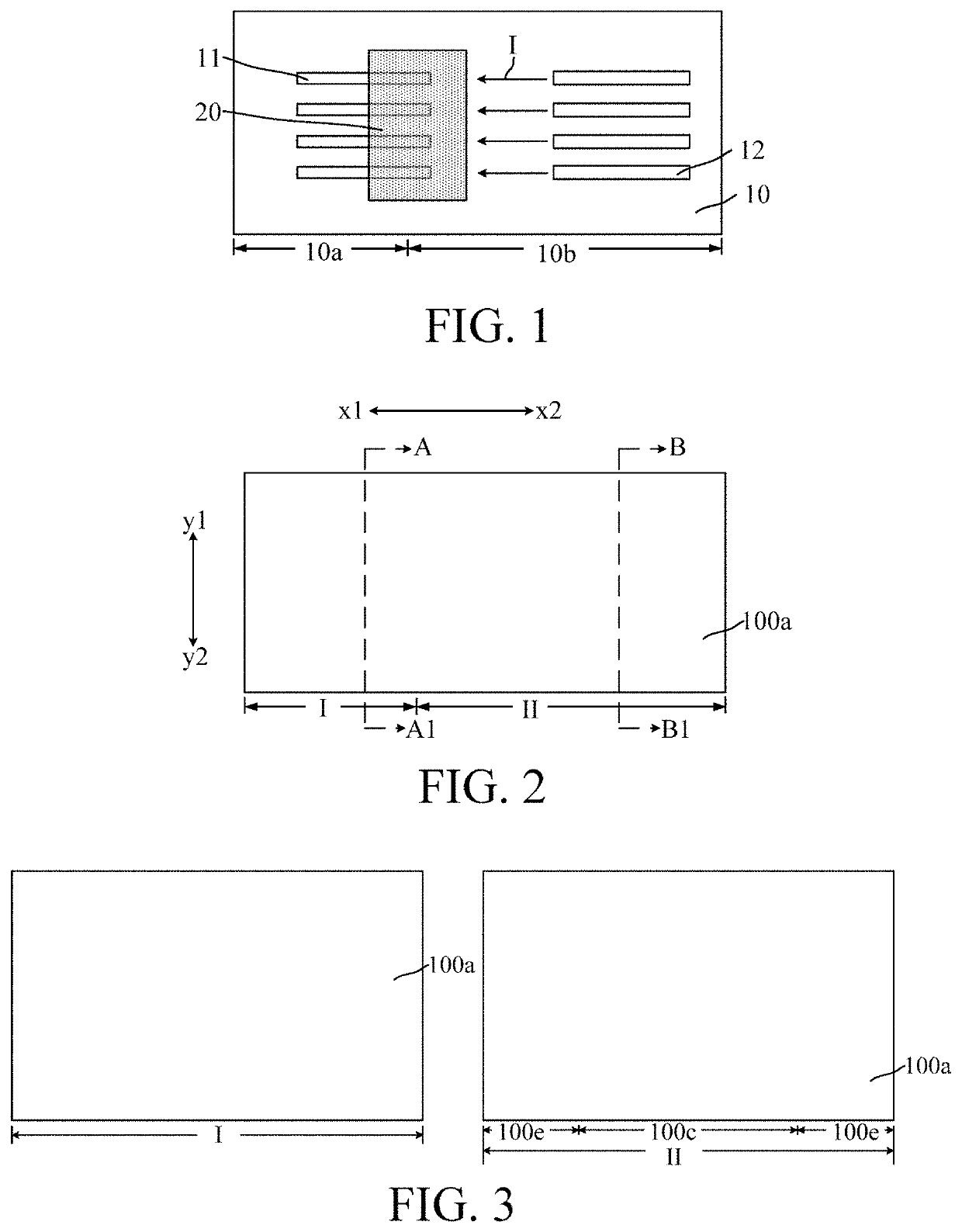
[0017]Referring to FIG. 1, FIG. 1 is a schematic structural diagram of a semiconductor structure.

[0018]The semiconductor structure includes: a substrate, including a first region 10a used to form a well region and a second region 10b used to form a drift region, where the first region 10a is adjacent to the second region 10b; fins (not marked), protruding out of the substrate 10, the fins include first fins 11 located at a junction of the first region 10a and the second region 10b, and second fins 12 located on the second region 10b; and a gate structure 20, located at the junction of the first region 10a and the second region 10b, where the gate structure 20 covers a partial top of the first fin 11, and a partial sidewall of the first fin...


PUM

PropertyMeasurementUnit
thicknessaaaaaaaaaa
widthaaaaaaaaaa
width W2aaaaaaaaaa

Abstract

A semiconductor structure and a method for forming a semiconductor structure are disclosed. A forming method may include: providing a base, including a first region used to form a well region and a second region used to form a drift region, where the first region is adjacent to the second region; and patterning the base, to form a substrate and fins protruding out of the substrate, where the fins include first fins located at a junction of the first region and the second region and second fins located on the second region, where the quantity of the second fins is greater than the quantity of the first fins. In some implementations of the present disclosure, the quantity of the second fins is increased to correspondingly increase the length of a flow path in which a current flows from a drain region to a source region, thereby reducing a voltage drop in the current flow path, and further improving a breakdown voltage of an LDMOS, to improve the device performance of the LDMOS.

Description

RELATED APPLICATIONS[0001]The present application claims priority to Chinese Patent Appln. No. 201811368055.2, filed Nov. 16, 2018, the entire disclosure of which is hereby incorporated by reference.BACKGROUNDTechnical Field[0002]Embodiments and implementations of the present disclosure relate to the field of semiconductor manufacturing, and in particular, to a semiconductor structure and a forming method thereof.Related Art[0003]As the use of semiconductor chips increases, factors that cause electrostatic damage to the semiconductor chips are also increasingly growing. In an existing chip design, an electrostatic discharge (ESD) protection circuit is generally used to reduce the chip damage. The design and application of the existing ESD protection circuit includes: a gate grounded N-type field effect transistor (Gate Grounded NMOS, GGNMOS for short) protection circuit, a silicon-controlled rectifier (SCR) protection circuit, a lateral double diffused field effect transistor (Later...

Claims


Application Information

Patent Timeline
Patent Type & Authority Patents(United States)
IPC IPC(8): H01L21/8234H01L29/78H01L21/308H01L29/66
CPCH01L29/7816H01L21/3086H01L21/823431H01L29/66681H01L29/7851H01L29/0611H01L27/0886H01L29/66795
Inventor ZHOU, FEI
Owner SEMICONDUCTOR MANUFACTURING INTERNATIONAL (BEIJING) CORP
Why Eureka
Try Eureka