
Backside metalization with through-wafer-via processing to allow use of high q bondwire inductances

a technology of backside metalization and through-wafer-via processing, which is applied in the direction of electrical equipment, semiconductor devices, semiconductor/solid-state device details, etc., can solve the problems of no known solution for using bond wires in wlcsp or flip-chip integrated circuit (ic) designs, and no way of connecting bond wires to on-chip circuitry

Active Publication Date: 2021-11-09
SKYWORKS SOLUTIONS INC
View PDF6 Cites 0 Cited by
  • Summary
  • Abstract
  • Description
  • Claims
  • Application Information

AI Technical Summary

Benefits of technology

The present invention provides a flip-chip integrated circuit die with through-wafer vias and a bond wire that electrically couples the vias at the rear side of the die. The bond wire may be an inductive element in a matching circuit for active circuitry or an inductive element in a matching circuit for a power amplifier. The active circuitry may include a radio frequency circuitry or a power amplifier. The electrical structure includes a first integrated circuit die and a second integrated circuit die with bond pads and at least one bond wire coupling them together. The technical effects include improved performance, reduced size, and improved reliability of the integrated circuit die.

Problems solved by technology

To date, there is no known solution for using bond wires in WLCSP or flip-chip Integrated Circuit (IC) designs.
Bumped chips are typically soldered to a laminate or printed circuit board (PCB) face down so there is no way of connecting bond wires to on-chip circuitry.

Method used


Image

  • Backside metalization with through-wafer-via processing to allow use of high q bondwire inductances
  • Backside metalization with through-wafer-via processing to allow use of high q bondwire inductances
  • Backside metalization with through-wafer-via processing to allow use of high q bondwire inductances

Examples


first embodiment

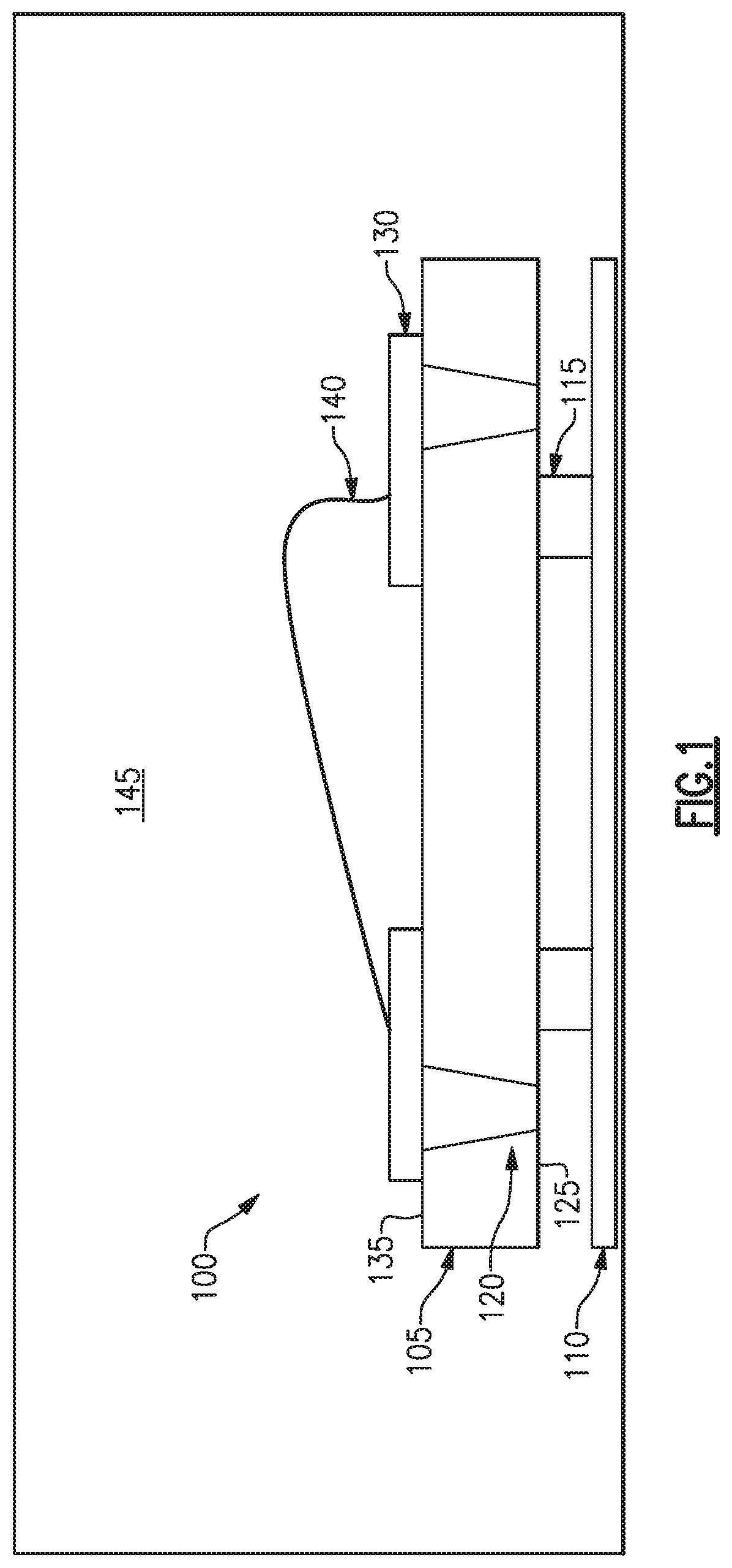
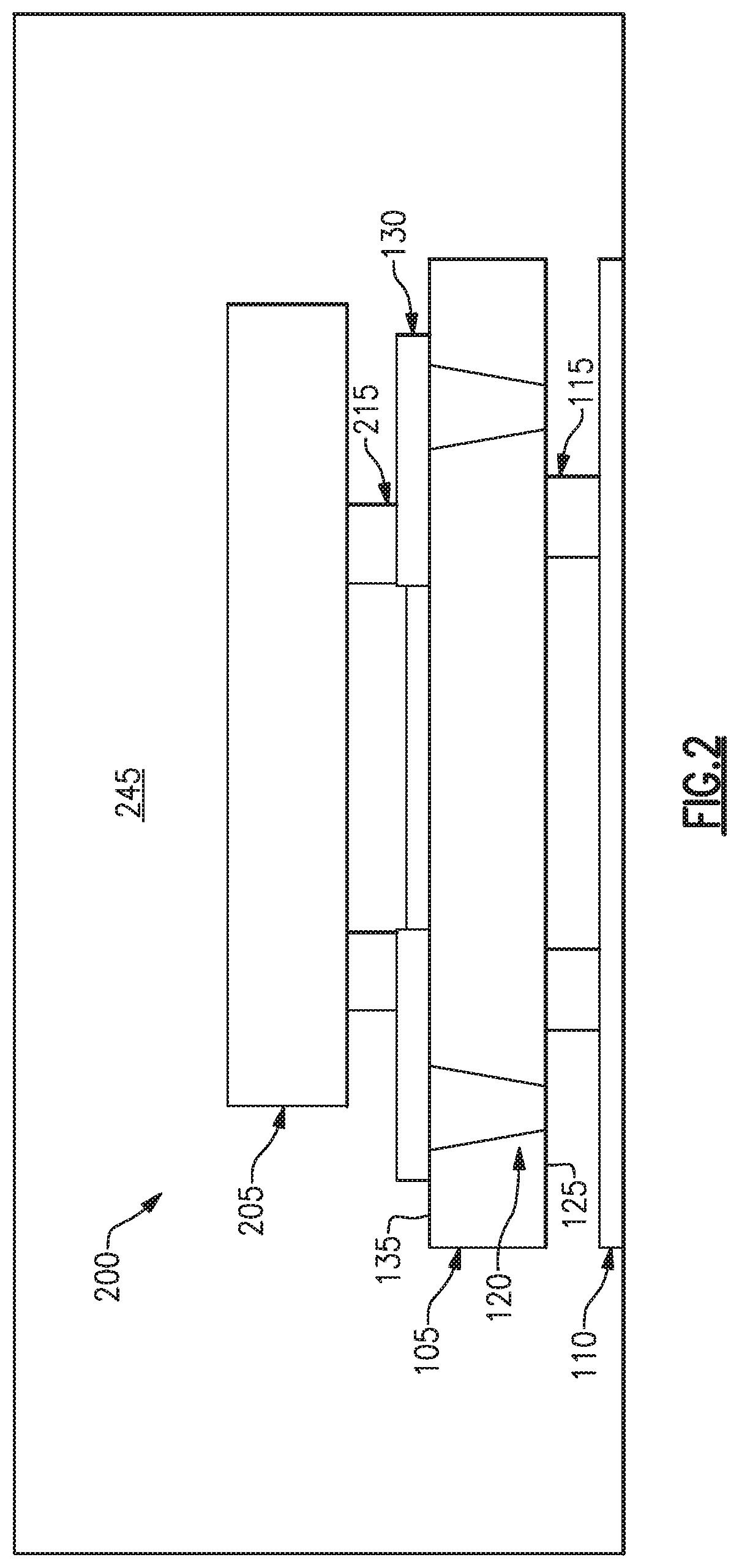
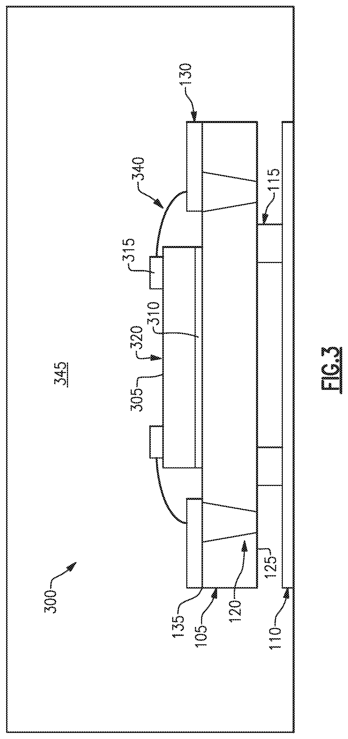
[0037]a flip-chip device as disclosed herein is illustrated in elevational view in FIG. 1, generally at 100. The flip-chip (or WLCSP) device 100 includes a chip scale package (CSP) die 105 flip-chip mounted to a substrate 110, for example, a printed circuit board or laminated substrate with conductive connectors 115, for example, copper pillars or solder balls. The conductive connectors 115 electrically and thermally connect bond pads (not shown) coupled to circuitry on the die 105 to substrate bonding pads (not shown) on the substrate 110, which in turn are coupled to electrical traces (not shown) for providing communication between the circuitry in the die 105 and external electronics, as well as for providing power to the circuitry in the die 105. The die 105 includes through-wafer vias 120 that may provide electrical and thermal communication between circuitry located within or at a front surface 125 of the die 105 and backend metallization 130 disposed on the rear 135 of the di...


PUM

PropertyMeasurementUnit
electrical structureaaaaaaaaaa
electronic structureaaaaaaaaaa
electricallyaaaaaaaaaa

Abstract

A flip-chip integrated circuit die includes a front side including active circuitry formed therein and a plurality of bond pads in electrical communication with the active circuitry, at least two through-wafer vias extending at least partially though the die and having portions at a rear side of the die, and a bond wire external to the die and electrically coupling the portions of the at least two through-wafer vias at the rear side of the die.

Description

CROSS-REFERENCE TO RELATED APPLICATIONS[0001]This application claims priority under 35 U.S.C. § 119(e) to U.S. Provisional Patent Application Ser. No. 62 / 490,766, titled “BACKSIDE METALIZATION WITH THROUGH-WAFER-VIA PROCESSING TO ALLOW USE OF HIGH Q BONDWIRE INDUCTANCES,” filed Apr. 27, 2017, which is incorporated by reference herein in its entirety.BACKGROUND1. Field of Invention[0002]The present invention relates generally to wafer level chip scale packages (WLCSP) and flip-chip designs including external bond wires.2. Discussion of Related Art[0003]To date, there is no known solution for using bond wires in WLCSP or flip-chip Integrated Circuit (IC) designs. Bumped chips are typically soldered to a laminate or printed circuit board (PCB) face down so there is no way of connecting bond wires to on-chip circuitry.SUMMARY OF INVENTION[0004]According to one aspect of the present invention there is provided a flip-chip integrated circuit die. The flip-chip integrated circuit die compr...

Claims


Application Information

Patent Timeline
Patent Type & Authority Patents(United States)
IPC IPC(8): H01L23/00H01L25/065H01L25/00H01L21/56H01L23/48H01L23/31
CPCH01L24/49H01L21/565H01L23/3114H01L23/481H01L24/09H01L24/48H01L24/73H01L25/0657H01L25/50H01L24/16H01L24/32H01L24/85H01L2224/02372H01L2224/02377H01L2224/04042H01L2224/04105H01L2224/056H01L2224/05548H01L2224/05568H01L2224/131H01L2224/13147H01L2224/16145H01L2224/16227H01L2224/2919H01L2224/32145H01L2224/45144H01L2224/4809H01L2224/4813H01L2224/48149H01L2224/4912H01L2224/73215H01L2224/73253H01L2224/73257H01L2225/06527H01L2225/06517H01L2225/06513H01L2225/06506H01L23/66H01L2223/6611H01L2223/6655H01L2924/014H01L2924/00014H01L2924/00012H01L2924/0665
Inventor GILL, BHARATJEET SINGHPOULIN, GRANT DARCY
Owner SKYWORKS SOLUTIONS INC
Learn More